
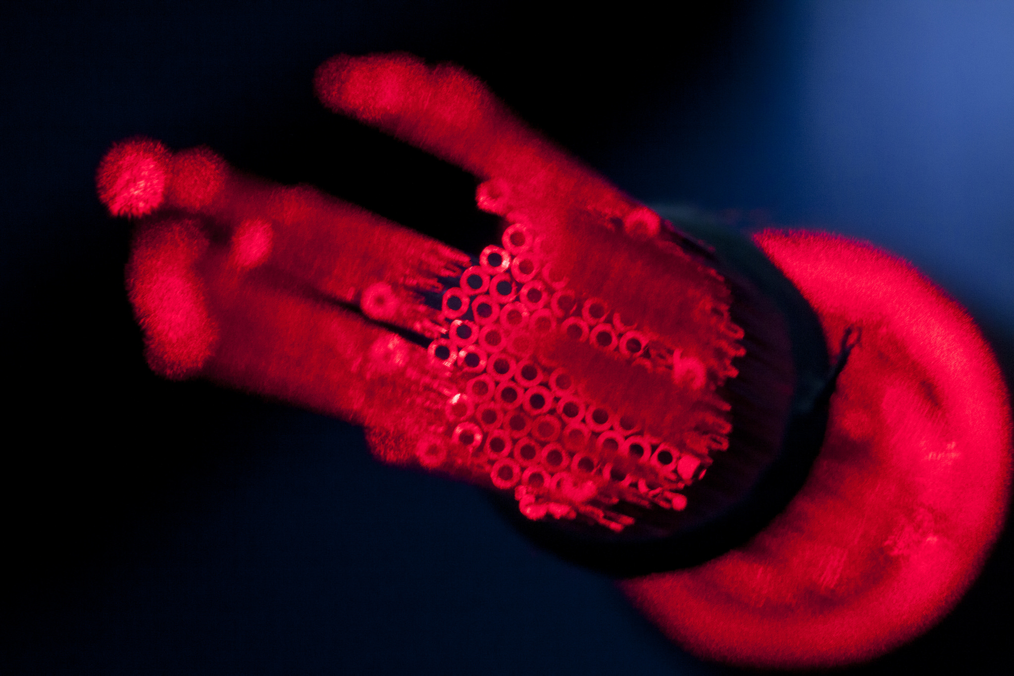
From photonic integrated circuits for AI datacenters to optical interferometers and quantum photonic systems, the AlGaAs/AlOx index contrast enabled by ALOXTEC is a key process for III-V waveguide integration.
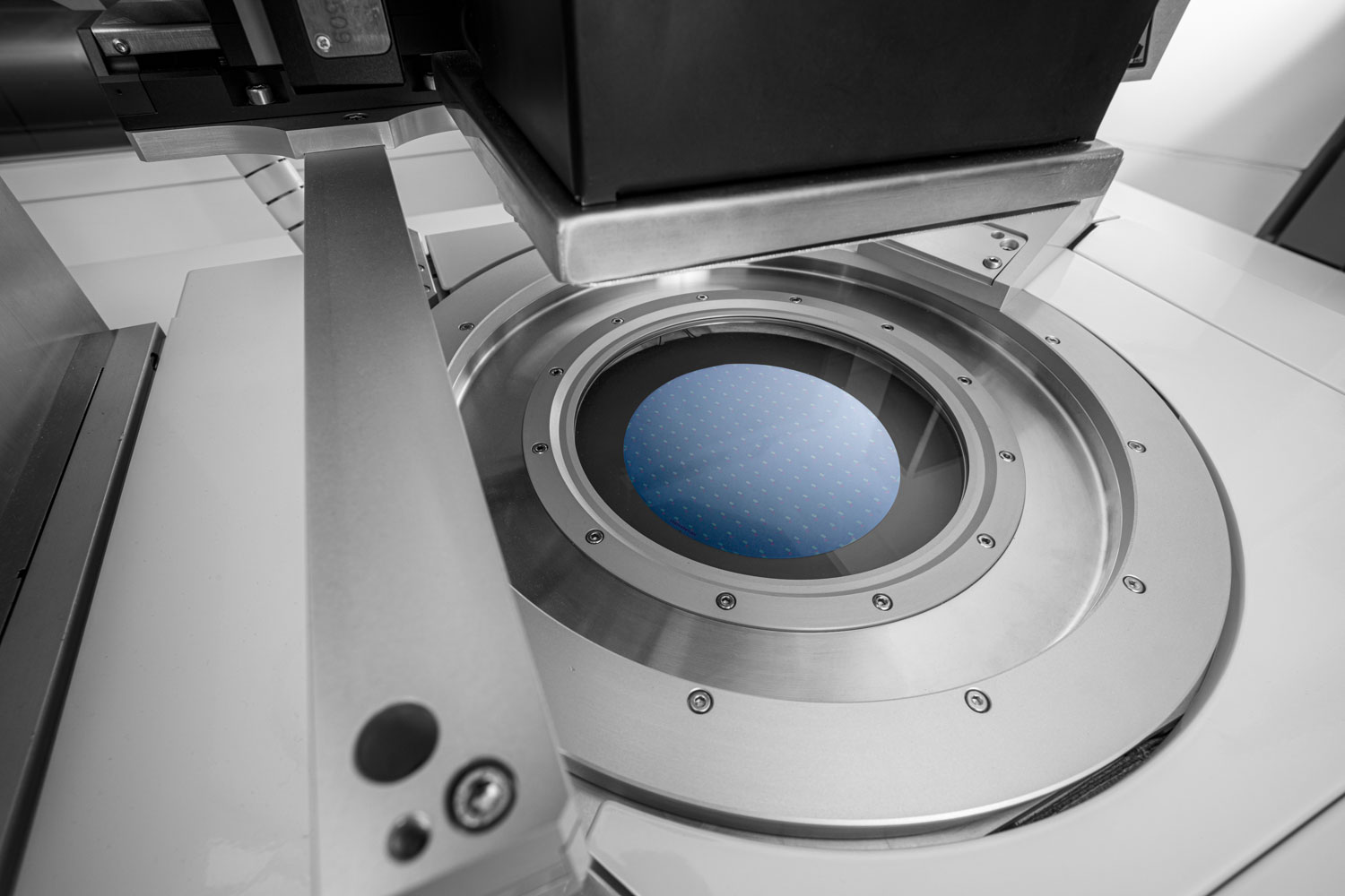
The ability to guide light efficiently in a semiconductor waveguide depends on index contrast: the larger the difference in refractive index between the waveguide core and its surrounding cladding material, the more strongly the optical mode is confined within the core, and the smaller the minimum waveguide cross-section that can be used without prohibitive radiation losses. In silicon photonics, the SiO₂/Si achieve highly confined waveguide widths and tight bending radii in passive integrated circuits. In III-V compound semiconductor systems based on GaAs/AlGaAs, the native index contrast between GaAs (n = 3.52) and Al0.3Ga0.7As (n = 3.27) is insufficient for the dense photonic integration required in advanced PICs, quantum photonic circuits, and high-efficiency non-linear optical devices.
Wet thermal oxidation of an AlAs or very-high-Al-content AlGaAs layer changes this constraint fundamentally. The conversion of AlAs to amorphous aluminium oxide (AlOx) produces a material with one of the largest index contrasts achievable in any semiconductor-compatible material system, comparable to the SiO2/Si contrast that has driven the success of silicon photonics, but now available within the III-V material system that provides the active gain, high-speed electro-optic modulation, and non-linear optical properties that silicon cannot replicate.
| Material | Refractive index (n) | Index contrast vs. AlOx | Waveguide role |
|---|---|---|---|
| GaAs | 3.52 | Δn = 1.92 | Core / active layer |
| Al0.3Ga0.7As | 3.27 | Δn = 1.67 | Cladding (moderate contrast) |
| AlOx (from AlAs oxidation) | 1.60 | Reference | Cladding (maximum contrast) |
| SiO2 (reference: silicon photonics) | 1.46 | Δn vs GaAs = 2.06 | SOI buried oxide |
The practical consequence of this index contrast is profound: AlGaAs/AlOx waveguides can confine optical modes in very tight cross-sections, enabling integration densities, bending radii, and coupling efficiencies that are entirely beyond the reach of AlGaAs/AlGaAs waveguides with native semiconductor cladding. For photonic integrated circuit designers, this means that the full toolkit of silicon photonics waveguide design, including ring resonators with radii of a few micrometres, directional couplers with tightly controlled coupling gaps, and multi-mode interference splitters with compact footprints, becomes accessible in a III-V material system that also integrates on-chip laser sources, amplifiers, and high-speed modulators.
The demand for high-index-contrast III-V waveguides is growing across four distinct application domains, each with specific requirements for oxidation depth precision, uniformity, and process reproducibility.

The exponential growth of AI training and inference workloads is driving a fundamental shift in datacenter interconnect architecture. Co-packaged optics (CPO), in which the optical transceivers are integrated directly alongside the GPU or switch ASIC, require photonic chips with sub-millimetre footprints capable of combining laser sources, modulators, wavelength multiplexers, and photodetectors on a single die. Silicon photonics currently dominates this space for passive functions, but its inability to generate light efficiently is a fundamental limitation. III-V/silicon heterogeneous integration, in which GaAs or InP gain chips are bonded or grown on silicon substrates and oxidation-defined waveguides connect the active and passive regions, is the leading approach to overcoming this limitation at scale.
For these hybrid III-V/silicon PIC architectures, the wet thermal oxidation step that defines the AlGaAs/AlOx waveguide cladding is a critical process. The AlOx layer must be formed with ultra-precise depth control to maintain the designed coupling efficiency between the III-V waveguide and the silicon photonics passive circuit. Any deviation in oxidation depth shifts the effective index of the III-V waveguide mode, detunes the phase-matching condition at the III-V/Si coupler, and reduces the optical transmission of the assembled PIC.

AlGaAs/AlOx waveguide systems are increasingly used as the basis for highly sensitive optical sensors, including evanescent-field biochemical sensors, integrated optical gyroscopes, and precision interferometers for displacement and refractive index measurement. In all these applications, the sensor sensitivity is a direct function of the effective index of the guided mode and its spatial derivatives with respect to the measurand. Precise control of the oxidation depth, which determines the lateral extent of the AlOx cladding and hence the effective index, is therefore a direct control handle on the calibrated sensitivity of the sensor device.
For integrated optical gyroscopes, where the phase accumulated per unit rotation rate is proportional to the enclosed area of the waveguide coil and to the effective group index of the guided mode, ultra-precise control of the AlOx cladding geometry translates directly into gyroscope scale factor accuracy. This level of process precision requires an oxidation system capable of real-time depth monitoring and automatic endpoint control rather than a conventional timed-oxidation approach.

Quantum photonic integrated circuits based on GaAs/AlGaAs represent one of the most technically demanding application areas for III-V wet oxidation. In these circuits, single-photon emitters (typically InAs quantum dots in a GaAs matrix) are coupled to AlGaAs/AlOx waveguides that route, split, and interfere single photons on-chip. The performance of the quantum photonic circuit is critically sensitive to two parameters that are directly controlled by the wet oxidation process: the optical loss of the AlOx-clad waveguide, which determines the maximum circuit depth before single-photon loss becomes prohibitive, and the geometric uniformity of the waveguide cross-section across the circuit footprint, which determines the phase accuracy of on-chip interferometers.
Quantum photonic applications therefore place the most stringent requirements of any III-V waveguide application on oxidation depth control and run-to-run reproducibility.

AlGaAs has one of the largest second-order non-linear optical coefficients of any material compatible with semiconductor fabrication, which is several hundred times larger than that of lithium niobate in its bulk form. AlGaAs/AlOx waveguides confine both the pump and signal fields within extremely small optical cross-sections, achieving modal overlap integrals and non-linear interaction lengths that enable efficient frequency conversion (second-harmonic generation, optical parametric amplification, difference-frequency generation) at pump powers accessible with on-chip laser sources. Applications range from on-chip optical clocks and frequency combs for precision metrology to mid-infrared sources for molecular spectroscopy and chemical sensing.
The process control requirements for III-V waveguide wet oxidation are, in several respects, more demanding than those encountered in VCSEL or EEL manufacturing. In III-V waveguide structures, the AlOx cladding must often be positioned within the evanescent tail of a guided mode whose lateral extent may be less than 3 µm, requiring strong depth control in the most demanding cases.
| Challenge | Physical origin | ALOXTEC solution |
|---|---|---|
| Ultra-Precise Oxidation Depth Control | Oxidation rate depends on local T, Al content and H2O delivery: timed processes cannot compensate in real time | Stop-on-Depth automation: real-time in-situ monitoring terminates the process at the exact target depth |
| Lateral uniformity across the full wafer for multi-waveguide PICs | Chamber temperature and H2O gradients create spatial variation in oxidation rate across the wafer surface | UniformPerf© delivers oxidation depth uniformity of min-max <±0.3 µm across 6-inch wafers, validated on photonic device structures |
| Run-to-run reproducibility for volume photonic device production | Chamber conditioning drift, water vapour delivery variation and thermal stabilisation tolerances accumulate into systematic depth offsets between lots | Closed-loop T/H/P process control and Stop-on-Depth automation produce run-to-run deviation of σ <0.1 µm on 6” wafers (With Uniformperf©) |
| Multi-EPI compatibility across complex photonic structures | Advanced photonic structures may include 3 to several hundred epitaxial layers with varying Al content: a single process recipe cannot be assumed to work across all structures | ALOXTEC T/H/P (Temperature/ Humidity/ Pressure) recipes have been proven across the full range of III-V photonic EPI structures, from simple AlAs single layers to complex multi-stack photonic crystal configurations |

The ALOXTEC wet thermal oxidation equipment range provides the process control capabilities required for III-V photonic waveguide fabrication across the full range of applications described above, from standard ridge-waveguide PICs to quantum photonic circuits and non-linear optical devices. The same T/H/P process architecture, in-situ vision system, and Stop-on-Depth automation that deliver industry-leading performance in VCSEL and EEL manufacturing are directly applicable to photonic waveguide oxidation, with process recipes proven across an extensive library of III-V photonic EPI structures.
The lateral extent of the AlOx cladding layer in a III-V waveguide structure is controlled by the same real-time in-situ monitoring and Stop-on-Depth automation that delivers Stop-on-Aperture control in VCSEL manufacturing. The ALOXTEC vision system tracks the advancing oxidation front continuously across the wafer surface, computing the lateral oxidation depth at every measured structure in real time. When the target depth is reached, the system terminates the process automatically, without operator intervention and without reliance on a pre-calibrated time constant.
This approach eliminates the systematic depth error that accumulates in timed-oxidation processes when the actual oxidation rate deviates from the calibrated nominal value due to EPI lot-to-lot Al content variation, chamber conditioning state, or water vapour delivery drift. For photonic waveguide structures where the target cladding depth may be specified to within 50 to 100 nm, this elimination of systematic error is not an incremental improvement: it is the difference between a process that reliably hits specification and one that requires post-process binning to recover acceptable yield.
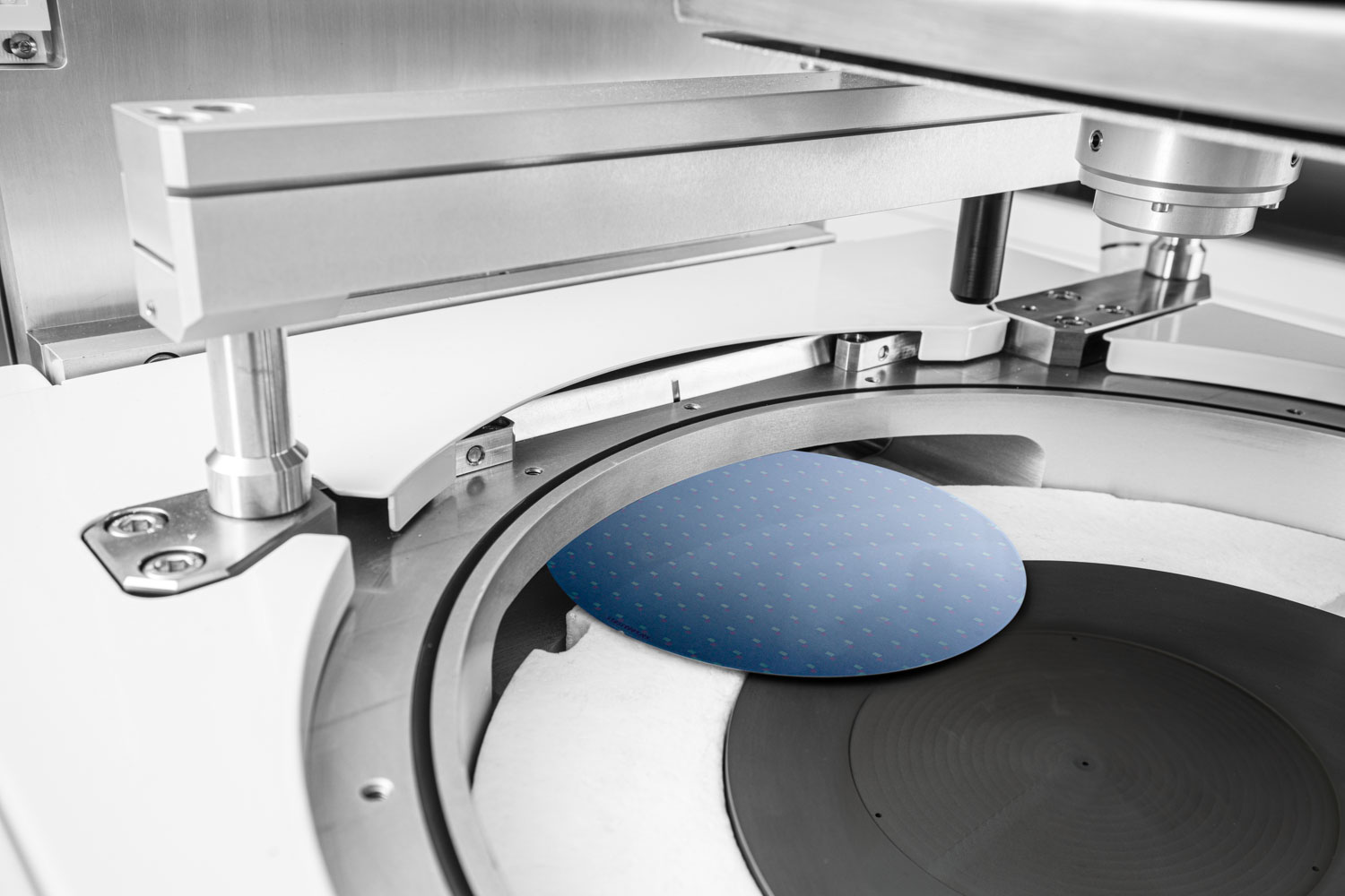
Photonic integrated circuits impose a uniformity requirement that is qualitatively different from the die-level yield requirement of discrete VCSEL or EEL manufacturing. In a PIC, multiple waveguide components, including ring resonators, directional couplers, and phase shifters, must maintain their designed phase and coupling relationships simultaneously across the full circuit footprint, which may span several square millimetres on a single die. Any spatial gradient in the oxidation depth across the wafer introduces a corresponding gradient in the effective index of the waveguides, creating a systematic phase error that accumulates across the circuit and degrades the performance of the integrated device.
UniformPerf© addresses this requirement directly. By delivering oxidation depth uniformity of min-max <±0.3 µm across 6-inch wafers, UniformPerf© ensures that the AlOx cladding geometry is consistent across the full wafer surface, enabling PIC designers to specify circuit performance without die-position-dependent corrections. For multi-chip photonic systems where identical PIC dies from different wafer positions must be matched in effective index and coupling coefficient, this wafer-level uniformity is a prerequisite for system-level yield.
Advanced III-V photonic structures present an oxidation process challenge that is largely absent in standard VCSEL manufacturing: the epitaxial stack may contain multiple AlAs or high-Al AlGaAs layers at different depths within the structure, with different thicknesses, different Al contents, and different intended oxidation depths. In a photonic crystal structure, for example, the Al-containing layers may number in the hundreds, and the oxidation of each layer must be controlled independently to avoid unintended modification of the optical structure.
The ALOXTEC Temperature / Humidity / Pressure ( T/H/P ) process space has been characterised across a broad range of III-V photonic EPI structures, including multi-layer photonic crystal slabs, coupled-resonator waveguide arrays, and hybrid III-V/Si integration stacks. The combination of the wide T/H/P ( Temperature / Humidity / Pressure) process window and the in-situ depth measurement capability allows process engineers to develop and qualify recipes for each specific EPI structure, with direct feedback on the oxidation depth and uniformity at every process run.

III-V photonic waveguide technology spans a development maturity range from fundamental academic research to early-stage commercial production. The ALOX GEN1.4L Manual and the ALOX GEN1.4L Auto provides the process flexibility and characterisation depth needed for research laboratory and device development environments.
The CHAROX 1.0 characterisation equipment provides dedicated oxide layer metrology for process validation in photonic integration flows, including automated depth mapping and uniformity analysis across the full wafer surface, without occupying the oxidation furnace chamber during measurement. For production environments where characterisation throughput is a bottleneck, the combination of in-furnace ALOXTEC characterisation and CHAROX metrology provides complementary coverage at different points in the production flow.
The ALOXTEC equipment capability for III-V photonic waveguide oxidation is grounded in a research partnership that predates the commercial photonics integration market by more than a decade. The scientific foundations of the ALOXTEC real-time in-situ monitoring approach were developed in collaboration with academic partners who were working on the fundamental physics of AlGaAs/AlOx waveguiding before it had a commercial application, and the engineering insights from that research are embedded in every aspect of the ALOXTEC equipment architecture.

The LAAS-CNRS laboratory in Toulouse, France, ALOXTEC’s founding scientific partner, has been one of the leading centres for research on wet thermal oxidation of III-V semiconductors for more than two decades. The LAAS team’s published work on the kinetics of AlAs lateral oxidation, the structural and optical properties of AlOx layers formed under different process conditions, and the relationship between process parameters and waveguide optical loss is the scientific bedrock on which the ALOXTEC process architecture was built. This ongoing collaboration ensures that new insights from the research community, including work on ultra-low-loss waveguide geometries, photonic crystal fabrication, and hybrid III-V/Si integration, are reflected in the process capabilities of current and future ALOXTEC equipment generations.

ALOXTEC furnaces deployed at the UC Berkeley Marvell NanoLab are used for III-V photonic waveguide research and device fabrication across a range of programmes, including quantum photonic circuits, non-linear optical devices, and III-V/Si integration systems. The Berkeley deployment represents a demanding validation environment: the Marvell NanoLab supports multiple research groups with different EPI structures and process targets, requiring the ALOXTEC equipment to demonstrate versatility and reproducibility across a wide range of waveguide geometries and oxidation conditions. The performance data accumulated at Berkeley constitutes an independent, peer-reviewed validation of the ALOXTEC equipment’s capability for III-V photonic waveguide applications.

The collaboration with Cardiff University focuses on advanced III-V oxidation processes for photonic device fabrication, including work on the formation and characterisation of AlOx layers in complex multi-stack EPI structures, the modelling of oxidation kinetics in confined geometries, and the development of new process protocols for emerging photonic integration architectures. Cardiff’s contributions to the understanding of oxidation front dynamics in photonic crystal and coupled-resonator structures are directly applicable to the process development challenges faced by customers working at the frontier of III-V photonic integration.
High-index-contrast III-V waveguide performance depends directly on the precision of the wet thermal oxidation step. Oxidation depth, uniformity and reproducibility determine optical confinement, effective index and phase stability across the circuit. The following questions address the key technical considerations for controlling waveguide oxidation at production scale.
 Save as PDF