

One process equipment. Four markets. Distinct requirements, common precision.
Wet thermal oxidation is the process step that defines the electro-optical identity of every VCSEL and EEL device. The oxide aperture it produces — its diameter, circularity, interface quality and wafer-level uniformity — determines the threshold current, emission wavelength, modulation bandwidth, beam quality and long-term reliability of the device. These parameters are not abstract specifications: they are the physical properties that make a VCSEL fit for purpose in a specific end application.
Each of the four markets served by ALOXTEC — consumer electronics and mobile, data centers and AI infrastructure, automotive LiDAR and intelligent mobility, and industrial sensing and healthcare photonics — translates those physical properties into a distinct set of manufacturing requirements. Volume, qualification framework, process documentation depth, yield economics and reliability expectations differ fundamentally across these four contexts. The ALOXTEC products are designed to address all four, from a single unified process and metrology architecture.

Consumer electronics is the highest-volume market for VCSEL-based photonic devices and, by many metrics, the most demanding manufacturing environment in which photonic components are produced. Structured light and time-of-flight 3D sensing systems, proximity sensors, AR/VR illuminators and wearable health monitors are embedded in billions of devices shipped annually. The combination of requirements — extreme production volumes, smallest device geometries, tightest cost targets and uncompromising reliability over millions of use cycles — pushes the wet oxidation step to its operational limits.
In this context, the primary manufacturing lever is aperture uniformity across the full wafer. At consumer electronics scale, a single percentage point of yield improvement on a 6-inch wafer translates into millions of additional good dies per year. Non-uniform apertures produce threshold current spread across VCSEL arrays, generating intensity non-uniformity in 3D sensing dot patterns and wavelength dispersion across proximity sensor channels. The ALOXTEC UniformPerf© option, delivering aperture uniformity min-max < 0.3 µm , and the 2026 wafer rotation and in-situ measurment innovation on the GEN1.4L Auto / GEN1.4L Manual / GEN2.0 HV Auto, significantly improve process uniformity.

Artificial intelligence has become the primary driver of growth in the optical interconnect market. Large-scale AI training and inference clusters require high-speed, short-reach optical links — based almost exclusively on VCSEL parallel optics over multimode fibre — in volumes that impose a fundamentally new demand pattern on the component supply chain: large-volume procurement events that must be fulfilled within tight commissioning windows, at bandwidth specifications that advance with each processor generation.
The wet oxidation step is critical on two dimensions simultaneously. Aperture control precision directly determines VCSEL modulation bandwidth: at 100 Gbps per lane and beyond, achieving the target bandwidth at the specified threshold current requires ultra-tight aperture size deviation control that timed oxidation cannot consistently deliver. Run-to-run aperture repeatability (σ < 0.1 µm with Stop-on-Aperture and UniformPerf©) translates into stable emission wavelength distributions across production lots, reducing WDM channel alignment risk at installation. In addition, zero-requalification recipe portability between the ALOX GEN1.4L Auto and the GEN2.0 HV Auto eliminates the qualification delay that would otherwise be incurred during production ramp-up.

Automotive LiDAR represents a fundamentally different manufacturing environment compared to consumer electronics or datacom. Performance alone is insufficient: reliability under extreme thermal, mechanical and operational conditions is a non-negotiable requirement. VCSEL devices must operate consistently over 10 to 15 years, across temperature ranges from −40°C to +125°C, under continuous or high-duty-cycle pulsed operation, while meeting AEC-Q102 qualification — the mandatory entry gate to the automotive supply chain.
The long-term reliability of an automotive LiDAR VCSEL is determined primarily at the wet oxidation step. Oxide layer delamination — the dominant field failure mode in high-power VCSELs under thermal cycling — originates from residual interfacial stress accumulated during oxidation, amplified by arsine entrapment at elevated chamber pressures. The ALOXTEC low-pressure process addresses this failure mechanism at its physical origin. Integrated post-oxidation annealing further reduces interfacial stress. The combination produces oxide layers with the stability required to pass AEC-Q102 thermal cycling, while the per-wafer aperture maps, circularity indices and SECS/GEM process traces provide the process documentation infrastructure required for automotive Tier 1 supplier qualification.
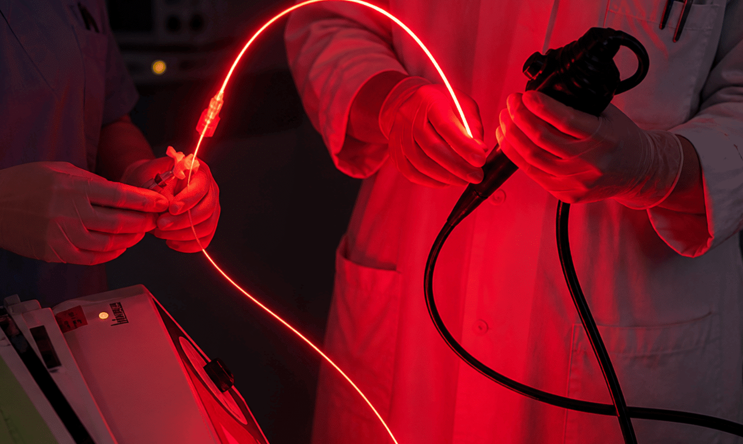
Industrial sensing and healthcare photonics together represent the most technically diverse segment of the VCSEL and EEL market. Applications span tunable diode laser absorption spectroscopy (TDLAS) for gas sensing, optical coherence tomography (OCT) for medical imaging, flow cytometry, high-power EEL-based therapeutic lasers and industrial range finding — each with distinct optical specifications but sharing a common process requirement: ultra-tight aperture size deviation control for emission wavelength stability, and full per-wafer process documentation for regulatory compliance.
Unlike consumer or datacom production, this sector combines low-to-medium volumes with high product diversity, frequent recipe changes across epitaxial structures, and strict regulatory frameworks — ISO 13485, FDA 21 CFR Part 820, IEC 60601 — that impose mandatory process traceability at the component level. The ALOXTEC portfolio equipment addresses this combination through its full T/H/P recipe flexibility, Stop-on-Aperture automation across all AlGaAs structures, in-situ wavelength mapping via the monochromator channel, and per-wafer characterisation output compatible with ISO 13485 and 21 CFR Part 820 documentation requirements.
The ALOXTEC equipment serves all four market sectors from a single process and metrology system. The same Stop-on-Aperture endpoint logic, the same dual-camera in-situ vision system, the same T/H/P process window, the same UniformPerf© uniformity option and the same SECS/GEM connectivity are common across the full equipment range — from the ALOX GEN1.4L Manual used in R&D and small-volume production to the ALOX GEN2.0 HV Auto deployed in high-volume consumer and datacom fabs.
This architectural consistency has a direct operational consequence for manufacturers serving multiple markets or scaling from one sector to another: process recipes, measurement data formats, operator training and qualification documentation are all transferable across tool generations and production scales without modification. A process developed for an industrial sensing application on the GEN1.4L Manual can be transferred to the GEN2.0 HV Auto for volume production without requalification. A recipe qualified for automotive LiDAR production generates per-wafer documentation in the same format as the same recipe running on a consumer electronics production line.

| Consumer Electronics & Mobile | Data Centers & AI Infrastructure | Automotive LiDAR & Intelligent Mobility | Industrial Sensing & Healthcare | |
|---|---|---|---|---|
| Primary VCSEL/EEL use | 3D sensing, ToF, proximity, AR/VR, wearables | Optical transceivers, parallel optics, CPO | Pulsed VCSEL arrays, FMCW LiDAR, ADAS | TDLAS, OCT, flow cytometry, range finding, therapeutic lasers |
| Volume profile | Very high (tens of millions of units/year) | Very high — step-change ramp events | Medium — but 100% qualification rate required | Low to medium — high product diversity |
| Primary manufacturing driver | Yield, cost per die, uniformity | Bandwidth, wavelength stability, ramp speed | Reliability (AEC-Q102), traceability, ASIL | Wavelength precision, process flexibility, regulatory compliance |
| Critical oxidation parameter | Aperture uniformity across full wafer | Aperture precision for bandwidth + WDM λ | Interface quality (low-pressure) + circularity | Aperture Size Deviation Control + Per-Wafer Traceability |
| Qualification standard | OEM supplier qualification | Hyperscale procurement specs / SECS/GEM | AEC-Q102 / IATF 16949 / ASIL | ISO 13485 / FDA 21 CFR Part 820 / IEC 60601 |
| Key ALOXTEC differentiator | UniformPerf© + Stop-on-Aperture at volume | Recipe portability GEN1.4 → GEN2.0, SECS/GEM | Low-pressure process + integrated annealing | Per-wafer data, recipe portability, λ mapping |
 Save as PDF