

About our Proprietary Real-Time In-Situ Monitoring in Wet Thermal Oxidation
Every wet thermal oxidation system can be described by the data it makes available and the moment at which it makes that data available. In a conventional timed furnace, process data consists of temperature, water flow and elapsed time: indirect indicators of what is happening to the wafer, available continuously but incapable of directly measuring the quantity that matters, which is the actual aperture size on the actual device structures. In the ALOXTEC system, process data includes the direct, real-time, spatially resolved measurement of the advancing oxidation front across the full wafer surface, available as the process unfolds, at the mesa level, without any interruption of the oxidation cycle.
This difference is the direct consequence of a hardware architecture that was designed from the ground up for in-situ optical metrology of wet thermal oxidation in III-V semiconductors. This page describes that architecture: its five components, their individual metrological capabilities, and how they function together as an integrated measurement system embedded within the furnace chamber.
The process control logic that this system enables, specifically the Stop-on-Aperture endpoint detection algorithm and its implications for yield, is described on the Oxide Aperture Control and In-Situ Monitoring page. The measurement outputs that the system generates and their role in process quality assessment are described on the Characterisation and Mapping page. The hardware architecture of ALOXTEC’s in-situ vision system, which enables Stop-on-Aperture, is described in detail on the Real-Time In-Situ Monitoring System page. This page focuses on the process control logic, the failure modes it eliminates, and its quantitative implications for yield and production stability.
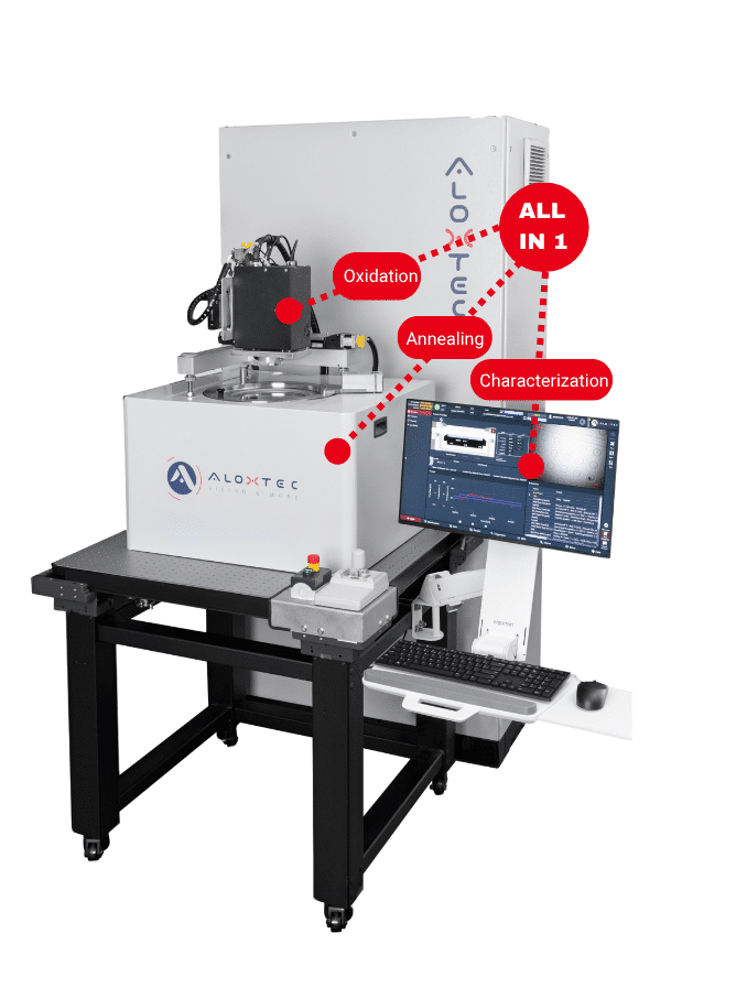
In the absence of in-situ monitoring, the state of a wafer during wet thermal oxidation is unobservable. The furnace chamber is sealed, the wafer is at process temperature, and the oxidation front is advancing laterally through the buried epitaxial layer with no external visibility. The only way to know what has happened is to complete the process, cool the wafer, remove it from the chamber, and measure it on a separate metrology tool.
This post-process approach has three structural limitations that constrain both yield and process development cycle time. First, any uniformity deviation, over-oxidation, or endpoint error is detected only after it has occurred, on a wafer that can no longer be corrected. Second, the metrology step adds cycle time, handling risk and equipment cost to every process run. Third, the feedback loop from measurement to process correction spans at least one full wafer cycle, meaning that systematic process drift can affect multiple wafers before it is detected and corrected.
ALOXTEC’s approach to this problem is architectural rather than incremental. Rather than improving the accuracy of post-process metrology or the calibration of timed oxidation models, the ALOXTEC system places a full optical measurement capability inside the furnace chamber itself, operating in real time throughout the oxidation run. This is not an add-on feature: it is the central design principle of the ALOXTEC technology, and every component of the vision system exists to serve this objective.
The metrological consequences of this design choice are significant. Process quality data is available before the wafer leaves the chamber. Uniformity gradients are detected as they develop, not after the run is complete. The endpoint decision is based on measured aperture size, not on a model prediction. And the post-oxidation characterisation sweep, which generates the full wafer-level measurement map, is performed within the same process cycle, without any additional handling or metrology step.
The ALOXTEC in-situ vision system consists of five hardware and software components, each with a distinct and non-redundant metrological function. They operate as an integrated system: the X/Y/Z system provides spatial access, the dual-camera configuration provides optical measurement at two spatial scales simultaneously, the monochromator extends the measurement to the wavelength domain, and the pattern recognition software converts optical images into quantitative metrology data in real time.
| System component | Technical function | Metrological capability |
|---|---|---|
| X/Y/Z motion system | Motorised three-axis positioning stage that moves the vision system above the wafer surface during the oxidation run. Provides full-wafer spatial coverage with programmable scan trajectories. | The X/Y/Z system is the fundamental enabler of full-wafer measurement. Unlike fixed-point monitoring systems, which measure oxidation at a single representative location, the ALOXTEC equipment scans freely across the entire wafer surface. This means that every monitored mesa contributes to the aperture map, not just a handful of reference sites. The resulting spatial resolution of the measurement reflects the mesa pitch of the actual device structure, not the sampling density of an external metrology tool. |
| Low-magnification camera | Wide-field optical channel providing a continuous wafer-level view throughout the oxidation run. Operates simultaneously with the high-magnification channel. | The low-magnification channel provides the spatial context for the wafer-level measurement: it captures the distribution of oxidation progress across the full wafer in real time, enabling the system to detect large-scale uniformity gradients as they develop during the run rather than after it is complete. This channel also provides the reference frame for positioning the high-magnification camera at specific mesa locations of interest. |
| High-magnification camera | High-resolution optical channel for mesa-level imaging. Resolves individual VCSEL or EEL mesa structures and tracks the advancing oxidation front with ultra-high spatial resolution and minimal aperture size deviation. | The high-magnification channel provides the measurement precision required for aperture size determination. It resolves the oxidation front position at the mesa sidewall with sufficient spatial resolution to track aperture closure with ultra-precise accuracy, enabling the Stop-on-Aperture endpoint detection described on the Oxide Aperture Control page. The dual-camera architecture allows both spatial levels to operate simultaneously: wafer-level context and mesa-level precision remain available throughout the entire process run. |
| Monochromator | Wavelength-selective optical element that isolates a narrow spectral band for imaging. Can be tuned to the emission wavelength of the VCSEL structure being processed. | The monochromator capability enables a qualitatively different class of measurement: it allows the system to image the optical emission of the VCSEL structures directly, in real time, during the oxidation run. As the oxide aperture forms and the effective refractive index of the cavity changes, the emission wavelength shifts. The monochromator captures this shift continuously, providing a real-time wavelength map across the wafer as a direct function of oxidation progress. This measurement requires no additional equipment, no wafer transfer and no interruption of the oxidation process. |
| Automatic pattern recognition software | Image processing and machine learning algorithms that identify mesa structures on the wafer surface, register their coordinates and dimensions, and track the advancing oxidation front at each mesa throughout the run. | Pattern recognition is the software layer that converts optical images into metrology data. At run start, the software automatically identifies all mesa structures on the wafer without manual template definition or operator input. During the run, it continuously computes the oxidation front position at each tracked mesa, extracts aperture diameter, circularity and oxidation depth, and feeds these values to the Stop-on-Aperture control algorithm. The absence of manual setup is a practical production requirement: in a high-throughput environment, per-wafer operator configuration is not compatible with the cycle time constraints of volume manufacturing. |
The integration of the vision system within the furnace chamber is a non-trivial engineering challenge. The system must operate reliably at proximity to process temperatures, in a water vapour and arsine-containing atmosphere, across process cycles of varying duration and temperature profile, without any maintenance intervention between runs.
The optical access to the wafer surface is provided through a viewport engineered to maintain optical clarity throughout the process window. The X/Y/Z motion system is designed for repeatability across thousands of positioning cycles, ensuring that the measurement coordinates registered at run initialisation remain accurate throughout the run and across successive process cycles. All mechanical and optical components in contact with the process environment are selected and qualified for compatibility with the thermal, chemical and mechanical requirements of wet thermal oxidation at the process conditions used in all the ALOXTEC equipment.

The most consequential architectural difference between the ALOXTEC vision system and alternative in-situ monitoring approaches is the distinction between full-wafer spatial coverage and fixed-point measurement. This distinction determines what the system can and cannot know about the state of the wafer during the process.
| Monitoring dimension | Fixed-point in-situ monitoring | ALOXTEC full-wafer in-situ monitoring |
|---|---|---|
| Spatial coverage | Single measurement point, or a small number of fixed locations on the wafer. Oxidation progress at the reference site is assumed to be representative of the full wafer. | Full wafer surface. The X/Y/Z system scans all monitored mesas across the wafer, providing a spatially resolved measurement of oxidation progress at every measured die. |
| Uniformity detection | Cannot detect wafer-level uniformity gradients in real time. Gradients are only revealed after post-process metrology on the completed wafer. | Uniformity gradients are detected as they develop during the run. Centre-to-edge and azimuthal oxidation rate differences are visible in real time, enabling immediate process feedback. |
| Endpoint decision basis | Process termination is triggered by the oxidation state at the reference site(s). If the reference site is not representative of the full wafer, the endpoint decision systematically misrepresents the actual aperture distribution. | Process termination is triggered based on the measured aperture at a set of representative reference mesas distributed across the wafer, ensuring that the endpoint decision reflects actual wafer-level oxidation progress. |
| Post-process metrology requirement | Full post-process metrology is required to characterise the oxide aperture distribution across the wafer. This adds cycle time, equipment cost and handling risk. | Complete wafer-level characterisation is performed within the oxidation cycle, before wafer unloading. Post-process metrology is not required as a standard step for process control. |
| Wavelength measurement | Not available in fixed-point configurations without additional dedicated metrology equipment and wafer transfer. | Real-time emission wavelength mapping across the wafer surface during the oxidation run, provided by the integrated monochromator channel. No additional equipment or wafer transfer required. |
The practical consequence of full-wafer monitoring is that the ALOXTEC system has access to the complete spatial distribution of oxidation progress across the wafer at every point in the run. This information is used for three distinct purposes: real-time endpoint detection via Stop-on-Aperture, real-time uniformity monitoring during the active oxidation phase, and complete post-oxidation characterisation at endpoint. None of these functions is available to a fixed-point monitoring system operating from a single or small number of reference sites.


The monochromator capability of the ALOXTEC vision system enables a measurement that is unique to the ALOXTEC equipment: the real-time, spatially resolved mapping of VCSEL emission wavelength across the wafer surface during the oxidation process itself.
As wet thermal oxidation converts the AlGaAs layer to AlOx, the effective refractive index of the VCSEL optical cavity changes. Because the resonant wavelength of the cavity is determined by the optical path length, which is a function of the effective refractive index integrated over the cavity depth, this change in refractive index produces a shift in the emission wavelength. By imaging the VCSEL emission through the monochromator at a sequence of wavelengths during the run, the system maps the local emission wavelength at each measured mesa as a function of oxidation progress.
The in-situ wavelength map has two distinct metrological functions that are not available from any post-process measurement.
First, it provides a real-time indicator of EPI quality variation across the wafer. Because the emission wavelength is determined by the cavity structure, local variations in emission wavelength at equivalent oxidation depths reflect local variations in the epitaxial layer thicknesses or compositions, revealing EPI non-uniformities that the oxidation depth map alone cannot distinguish from process-induced variations.
Second, it enables direct process control for wavelength-sensitive applications. In datacom VCSELs designed for specific WDM channels, the emission wavelength must fall within a defined window to ensure channel alignment in the deployed optical system. The ability to monitor wavelength in real time during oxidation, and to correlate it with the aperture size measurement, gives process engineers a direct handle on the wavelength-aperture relationship for each specific epitaxial structure, without requiring a separate post-process wavelength mapping step.

Full SECS/GEM connectivity is available on the ALOX GEN1.4L Auto and GEN2.0 HV Auto systems. SECS/GEM (SEMI Equipment Communications Standard / Generic Equipment Model) is the industry-standard protocol suite for communication between semiconductor manufacturing equipment and the fab host system (Manufacturing Execution System, MES). Its implementation on the ALOXTEC equipment portfolio enables the system to participate fully in automated, host-controlled production environments characteristic of Tier 1 semiconductor manufacturing.
The SECS/GEM interface is not a data logging add-on. It is the mechanism through which the ALOXTEC system is integrated as a node in the fab’s production automation infrastructure, with bidirectional communication for recipe management, process control and real-time data streaming.
| Function | Production line integration benefit | |
|---|---|---|
| SEMI E30 (GEM) | Generic Equipment Model. Defines the standard behaviour of semiconductor manufacturing equipment with respect to host communication, state machine management and event reporting. | Ensures that the ALOXTEC system presents a predictable, standardised interface to the fab host system (MES). Equipment onboarding time is reduced and integration risk is minimised, because the equipment behaviour conforms to a known standard rather than requiring custom protocol development. |
| SEMI E37 (HSMS) | High-Speed Message Services. Defines the transport layer protocol for SECS-II messages over TCP/IP. | Enables high-throughput, low-latency communication between the ALOXTEC system and the fab host. Real-time process and measurement data can be streamed to the MES without communication bottlenecks that would compromise data completeness or timeliness. |
| SEMI E40 | Standard for Processing Management. Defines how process jobs, control jobs and recipes are managed and communicated between the equipment and the host. | Automated recipe loading from the fab host eliminates manual recipe selection at the tool, removing a potential source of operator error in production. The correct process recipe is loaded automatically based on the lot traveller, without operator intervention. |
| SEMI E42 | Recipe Management. Defines the standard for recipe upload, download, validation and management between equipment and host. | Process recipes can be managed centrally at the fab level, ensuring that all ALOXTEC systems in the production line run validated, version-controlled recipes. Recipe changes are propagated and tracked through the standard management layer. |
Beyond recipe and alarm management, the SECS/GEM interface enables continuous, real-time streaming of process and measurement data to the fab MES during the oxidation run. This includes process parameter traces (temperature, water flow, chamber pressure as functions of time), real-time aperture measurement data as generated by the vision system, and the complete post-oxidation characterisation dataset at endpoint.
The availability of this data stream at the MES level enables process traceability at the individual wafer level, lot-level statistical process control on aperture uniformity and run-to-run repeatability, and automated downstream lot disposition based on in-situ measurement results. For Tier 1 VCSEL manufacturers operating fully automated production lines, this integration capability is a prerequisite for deploying the ALOXTEC equipment in a volume production environment.

The in-situ vision system described on this page is integrated aacross the full ALOXTEC machine range. The same core optical measurement architecture, X/Y/Z system, dual-camera configuration, monochromator and pattern recognition software, is present in all four ALOXTEC equipment. This architectural consistency has a direct consequence for process development and technology transfer: a process characterised on the ALOX GEN1.4L Manual in a research environment generates the same categories of measurement data, in the same format, as the same process running on the ALOX GEN2.0 HV Auto in volume production.
The metrological outputs of the vision system, the five measurement maps generated at process endpoint, and their role in process quality assessment and yield management, are described in detail on the Characterisation and Mapping page.

Real-time in-situ monitoring fundamentally changes how wet thermal oxidation is controlled in production environments. By measuring the actual state of the wafer during the process, rather than inferring it from indirect parameters, it enables a shift from predictive to deterministic process control. The following questions address the principles, limitations and advantages of in-situ monitoring technologies.
 Save as PDF