

Discover how ALOXTEC’s process improves the performance of VCSELs in consumer electronics and mobile devices.
Consumer electronics is the largest volume application for VCSEL technology and, by many metrics, the most demanding manufacturing environment in which photonic components are produced. The combination of requirements imposed by this market, highest production volumes, smallest device geometries, tightest cost targets, and uncompromising reliability over millions of use cycles, pushes every step of the VCSEL fabrication process to its operational limits. Wet thermal oxidation is no exception.
This page translates the requirements of the consumer electronics market into their specific consequences for VCSEL wet oxidation process control, and maps those consequences to the capabilities of ALOXTEC’s equipment portfolio. It is written for process and engineering leaders at VCSEL component manufacturers whose customers include consumer electronics OEMs, and for technical decision-makers evaluating wet oxidation equipment for consumer-facing VCSEL production.
For a detailed technical description of the VCSEL wet oxidation process itself, see the VCSEL Wet Thermal Oxidation application page. For the process control technologies that enable yield and reliability at consumer electronics scale, see the Oxide Aperture Control and UniformPerf© technology pages.

VCSEL-based photonic modules are embedded in billions of consumer devices shipped annually. Structured light and time-of-flight 3D sensing systems for facial recognition are standard features across the premium smartphone segment worldwide. Proximity and ambient light sensors appear in virtually every smartphone and tablet. Wearable heart rate and blood oxygen monitors have migrated from medical devices to mass-market smartwatches. Augmented reality headsets, still an emerging category, are already consuming VCSEL arrays at volumes that stress the capacity of the component supply chain.
Each of these applications places a photonic module at the intersection of consumer electronics economics and photonic device physics. The photonic performance requirements are set by the application. The cost requirements are set by the bill-of-materials pressure of a consumer product manufactured at tens of millions of units per year. The reliability requirements are set by the expectations of consumers who return defective products and the warranty obligations of OEMs who absorb the cost. Meeting all three simultaneously is the defining challenge of consumer VCSEL manufacturing.
In consumer electronics VCSEL manufacturing, yield is not an abstract process metric. It is the direct determinant of component cost, and component cost is directly visible in the economics of supply agreements. At the scale of a high-volume consumer electronics supply chain, a single percentage point of yield improvement on a 6-inch wafer translates into millions of additional good dies per year, and millions of good dies at consumer pricing translate into commercially significant cost reductions per unit. The pressure to maximise first-pass yield at every process step, and to sustain that yield consistently across high-volume production campaigns, is continuous and intensifying as device geometries shrink and specification windows narrow.
The consumer electronics market encompasses a range of VCSEL applications that differ significantly in their specific requirements for aperture size, uniformity, wavelength control and reliability. The table below maps each major application to the VCSEL technology it uses and the specific manufacturing requirement it imposes on the wet oxidation step.
| Application | VCSEL technology | Manufacturing requirement imposed on wet oxidation |
|---|---|---|
| 3D facial recognition (structured light and time-of-flight) | VCSEL array illuminator: hundreds of emitters per module, precise aperture uniformity required for beam pattern quality. | Aperture uniformity across the full array determines the spatial uniformity of the illumination pattern. Non-uniform apertures produce threshold current spread across the array, causing individual emitters to turn on at different drive currents and generating intensity non-uniformity in the projected dot pattern. For structured light systems, dot pattern uniformity is directly linked to depth mapping accuracy. |
| Proximity and ambient light sensing (in-display sensors) | Single or small-array VCSEL emitter operating at low power with precise wavelength control for rejection of ambient light interference. | Emission wavelength must fall within a defined spectral window to ensure effective rejection of ambient light by the receiver filter. Aperture size directly controls emission wavelength through the effective refractive index of the cavity. Aperture size deviation control is required to maintain wavelength within the filter passband across all production units. |
| Heart rate and SpO2 monitoring (wearables and smartwatches) | VCSEL emitter at 850 nm or 940 nm for photoplethysmography. Reliability over millions of operating cycles at body contact. | Long-term reliability under repeated thermal cycling from body temperature to storage temperature is a primary specification. Oxide layer delamination is the dominant failure mode. Low-pressure oxidation and integrated post-oxidation annealing, as implemented in the ALOXTEC process, are required to produce oxide layers that sustain the required operational lifetime. |
| Augmented reality and mixed reality (near-eye displays and depth sensing) | High-density VCSEL arrays for structured light depth sensing and near-eye display illumination. Smallest possible device footprint with maximum aperture circularity. | AR devices impose the most demanding combination of requirements: smallest aperture dimensions, highest uniformity requirements for array-level beam quality, and extreme reliability targets for a wearable device expected to operate continuously for years. These requirements simultaneously demand Stop-on-Aperture precision, UniformPerf© uniformity, and low-pressure reliability process. |
| Gesture recognition and touchless interfaces (consumer devices and appliances) | VCSEL-based ToF sensing at range. Moderate precision requirements but high volume and low cost-per-unit targets. | Cost per good die is the primary economic driver. Yield maximisation at high volume is the direct manufacturing objective. Aperture uniformity across large-format wafers determines the fraction of dies meeting specification and therefore the unit cost of every shipped sensor module. |
The most demanding consumer VCSEL applications, particularly augmented reality near-eye displays and advanced 3D sensing systems for the next generation of smartphones, no longer impose individual requirements in isolation. They converge: small apertures, tight uniformity, precise wavelength control and high reliability are simultaneously required on the same device, manufactured at high volume. This convergence means that no single process optimisation addresses the full set of requirements. The Stop-on-Aperture endpoint control, the UniformPerf© uniformity option and the low-pressure reliability process of the ALOXTEC portfolio must operate together to meet the complete specification.

The consumer electronics market imposes four distinct and simultaneous manufacturing pressures on VCSEL wet oxidation equipment. Each pressure has a specific origin in market dynamics and a specific technical consequence for the oxidation process. The ALOXTEC equipment is engineered to address all four.
| Manufacturing pressure | Origin in the consumer electronics market | Direct consequence for VCSEL wet oxidation |
|---|---|---|
| Maximum yield at wafer scale | Consumer electronics supply chains operate on bill-of-materials economics where the cost of every individual component is scrutinised at the unit level. VCSEL modules are cost-sensitive components: even a single yield point per wafer has a measurable impact on the economics of a volume supply agreement. | Aperture uniformity is the primary yield lever at the oxidation step. Every die that falls outside the aperture specification window is lost yield with no recovery path. Achieving and sustaining ±0.3 µm aperture uniformity on 6-inch and 8-inch wafers with UniformPerf© is the most direct available lever for yield improvement at the oxidation step. |
| High-volume throughput with consistent quality | Consumer electronics product launches impose aggressive ramp schedules. A new smartphone generation may require tens of millions of VCSEL modules within weeks of launch. Production capacity must be available at scale, and quality must be consistent from the first wafer to the millionth. | Run-to-run repeatability is as important as single-run uniformity. The ALOXTEC Stop-on-Aperture function ensures that every run terminates at the same aperture diameter regardless of chamber conditioning drift or EPI lot variation. The σ < 0.1 µm run-to-run deviation with UniformPerf© is the production stability metric that sustains consistent quality across high-volume ramps. |
| Smallest aperture dimensions | Miniaturisation is a continuous pressure in consumer electronics. As VCSEL array densities increase and device footprints shrink, aperture diameters decrease. Single-mode VCSELs for AR and advanced 3D sensing applications require apertures below 5 µm. | Small aperture targets are the most sensitive to process variability.
Stop-on-Aperture capability down to less than 3 µm is a hard technical requirement for next-generation consumer VCSEL devices. |
| Long-term reliability in wearable environments | Wearables operate in uniquely demanding environments: continuous thermal cycling between body temperature and ambient, exposure to sweat and humidity, mechanical vibration from daily activity, and operational lifetimes measured in years. Component reliability specifications reflect these conditions. | Oxide layer reliability under thermal and mechanical cycling is the critical process quality dimension. Low-pressure oxidation and integrated post-oxidation annealing in the ALOXTEC process produce oxide layers with significantly lower interfacial stress than conventional high-pressure processes, directly improving resistance to delamination under the thermal cycling conditions of wearable use. |

In consumer electronics VCSEL production, the cost of a process excursion scales with volume. A wet oxidation run that produces out-of-specification aperture sizes on a significant fraction of dies is not a recoverable event at consumer scale. There is no rework path for a VCSEL die with an incorrect aperture diameter. The loss is immediate, total and proportional to the number of affected dies.
This is why the combination of Stop-on-Aperture endpoint control, which eliminates mean aperture error, and UniformPerf© uniformity, which eliminates spatial aperture spread, is not simply a performance improvement in a consumer electronics context. It is a risk reduction architecture. It replaces a process in which aperture errors are possible and their economic impact is unbounded, with a process in which the aperture outcome is deterministic and the risk of yield loss from oxidation variability is structurally minimised.

Consumer electronics VCSEL products follow a development cycle that starts in a research or pre-production environment and must transfer to volume manufacturing at a pace dictated by OEM product launch schedules. Any process requalification requirement at the transition from development to production introduces delay, engineering cost and yield risk at the moment of highest time pressure.
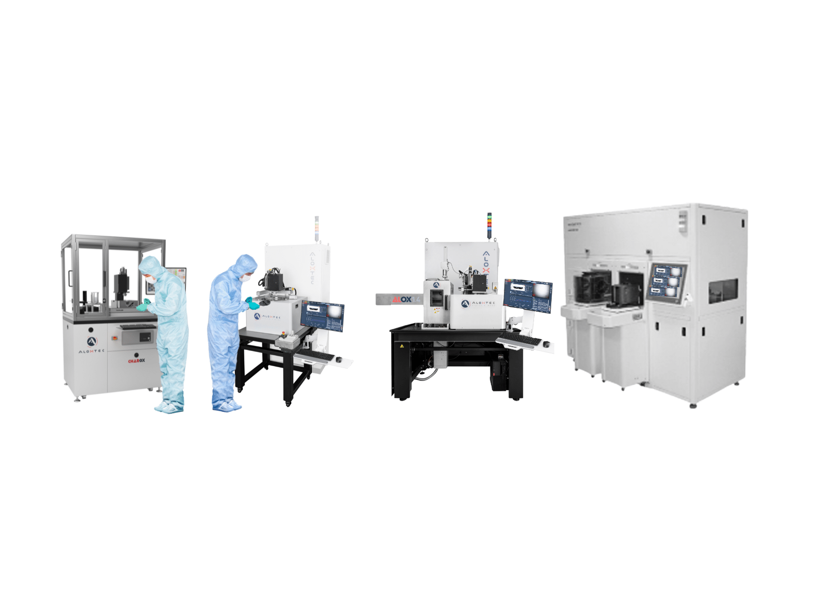
The ALOXTEC equipment range is designed to eliminate this transition cost. The ALOX GEN1.4L Manual and GEN1.4L Auto share the same oxidation process chamber architecture and in-situ vision system as the GEN2.0 HV Auto. Every process recipe developed on the development system transfers directly to the production system without modification and without requalification. The aperture targets, the Stop-on-Aperture parameters, the UniformPerf© configuration and the post-oxidation characterisation protocol are all portable across the machine range.
For a consumer electronics supply chain operating under OEM launch pressure, this portability is a commercial advantage as well as an engineering one. It means that process qualification work done during product development directly contributes to production readiness, with no duplicated effort and no validation gap at the machine transition.
For consumer electronics VCSEL applications where aperture uniformity is a primary yield driver, ALOXTEC recommends UniformPerf© as a configuration on all production equipment. The performance improvement from ±0.6 µm to ±0.3 µm min-max on 6-inch wafers, and from σ < 0.2 µm to σ < 0.1 µm run-to-run, is validated on Tier 1 VCSEL production wafers and transfers directly to consumer electronics epitaxial structures without additional process development. For applications with aperture specifications tighter than ±5 µm, UniformPerf© is in practice a technical requirement rather than an optional upgrade.
ALOXTEC’s expertise in VCSEL manufacturing for consumer electronics is built on a combination of advanced process control technologies and a strong production track record across high-volume photonic device manufacturing environments. The following questions address the key challenges faced by manufacturers operating at consumer electronics scale.
 Save as PDF