
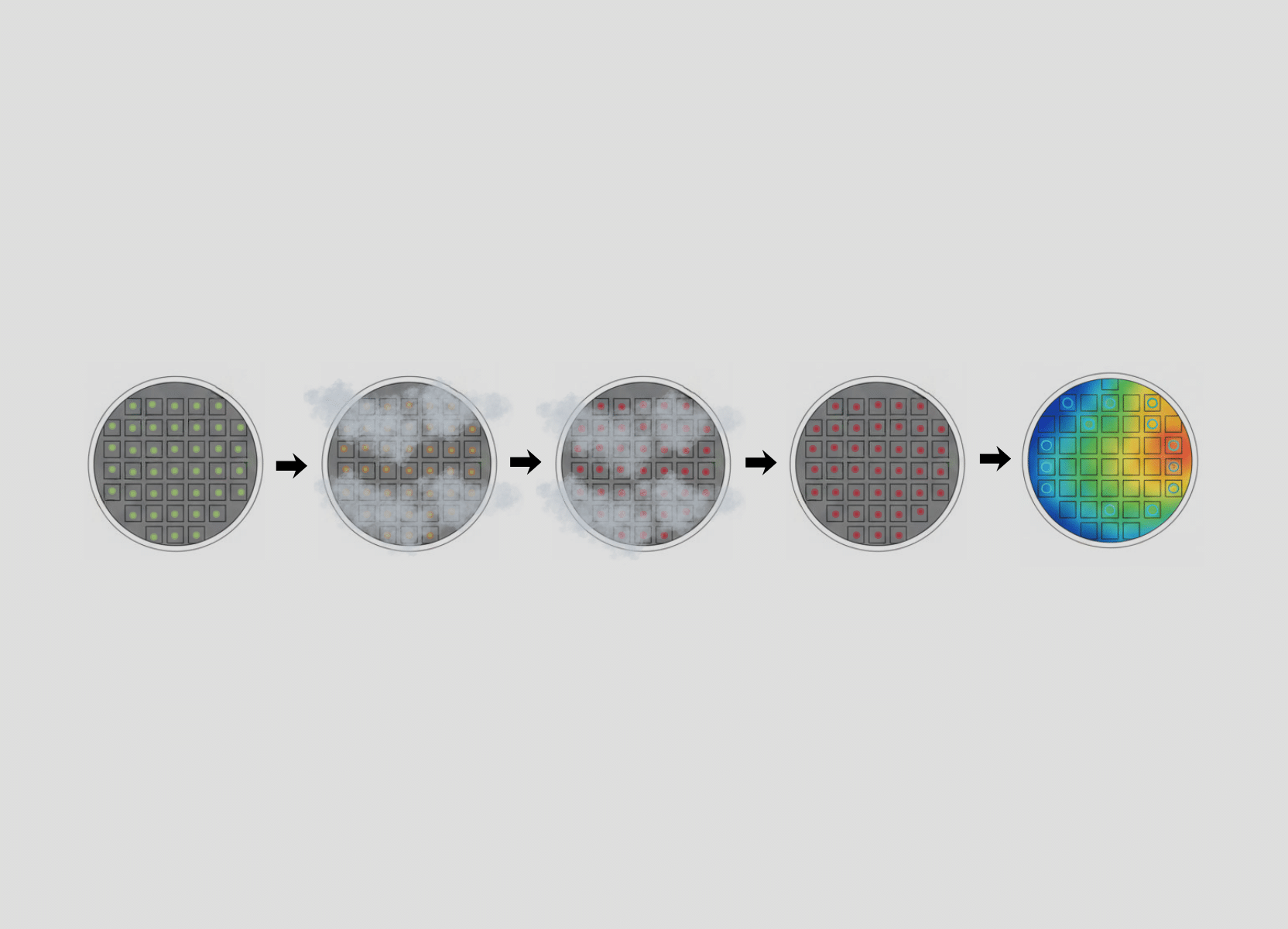
Wet oxidation process, real-time aperture control, in-situ metrology and spatial uniformity. One integrated equipment. Five technology domains.

Wet thermal oxidation converts a buried AlAs or high-Al-content AlGaAs layer into amorphous aluminium oxide (AlOx) through a vapour-phase reaction at elevated temperature. The oxidation front advances laterally from the exposed mesa sidewalls, producing the oxide aperture that defines current confinement and optical mode guidance in every device built on this process.
The reaction is governed by three interdependent parameters — temperature (T), water vapour flow (H) and chamber pressure (P) — whose combined effect on oxidation kinetics, oxide microstructure and aperture geometry cannot be decomposed independently. Low-pressure operation, a defining characteristic of the ALOXTEC process window, enables efficient arsine outgassing at the reaction front, producing a denser, more homogeneous oxide with demonstrably superior resistance to interfacial delamination under accelerated reliability testing.
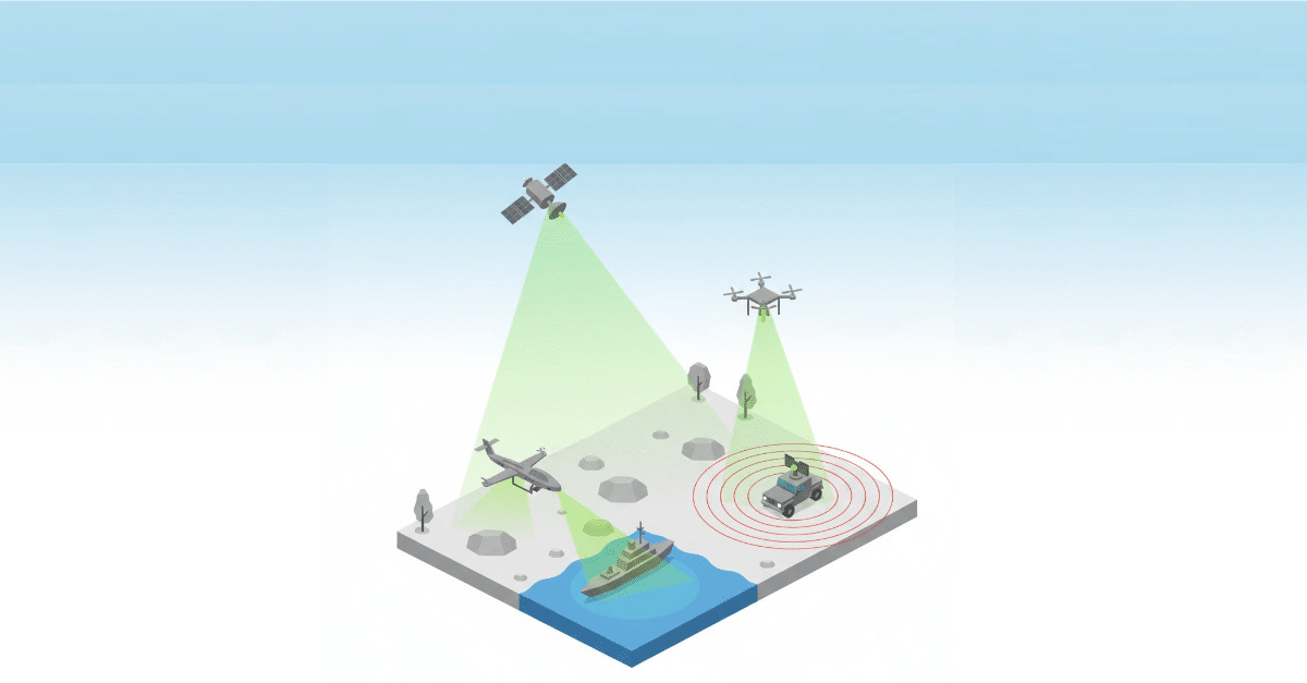
In VCSEL and EEL manufacturing, a deviation of a few tenths of a micron from the target aperture diameter shifts a device outside its electro-optical specification. Conventional time-based oxidation cannot compensate for run-to-run variability in epitaxial aluminium content, chamber conditioning state or local temperature gradients — any of which can move the oxidation rate outside the window a calibrated time endpoint was designed for.
The ALOXTEC Stop-on-Aperture system monitors the advancing oxidation front in real time across the full wafer surface and terminates the process at the exact target aperture diameter — on every run, regardless of incoming wafer variability. It operates without a device-specific calibrated rate model, adapting automatically to the actual oxidation behaviour of each wafer.

Stop-on-Aperture endpoint control and full wafer characterisation at process end both depend on a single architectural choice: placing a complete optical measurement system inside the furnace chamber, operating in real time throughout the oxidation run. In the absence of in-situ monitoring, the state of a wafer during oxidation is unobservable until the process is complete and the wafer is removed.
The ALOXTEC vision system integrates five components — a motorised X/Y/Z system, a dual-camera configuration operating at two spatial scales simultaneously, a monochromator for real-time VCSEL emission wavelength mapping, and automatic pattern recognition software — into a measurement architecture that is identical across the full ALOXTEC product range, from the GEN1.4L Manual to the GEN2.0 HV Auto.
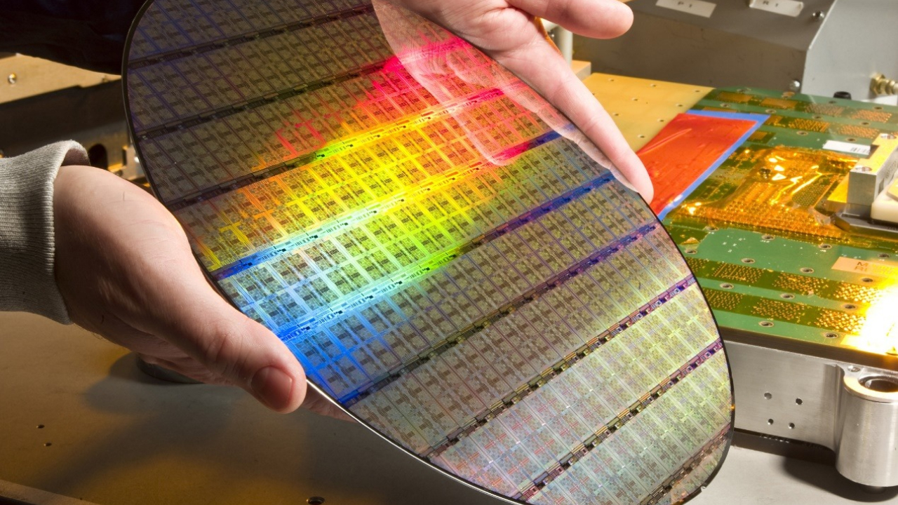
At the end of each oxidation run, the ALOXTEC vision system performs a complete wafer-level characterisation sweep in-chamber, before wafer unloading, without any additional metrology step or wafer transfer. This sweep generates five independent measurement maps: oxidation depth, aperture diameter, circularity index, mesa dimensions and VCSEL emission wavelength.
Each map provides non-redundant process quality information. The wavelength map in particular reveals epitaxial non-uniformities that the oxidation depth map alone cannot distinguish from process-induced variation — a metrological function unavailable from any post-process measurement sequence. The CHAROX 1.0 characterisation station extends this capability to QC workflows, incoming EPI inspection and non-ALOXTEC wafers.

Stop-on-Aperture controls the mean aperture diameter. It does not, by itself, eliminate the spatial gradient of aperture sizes across the wafer — a distinct physical problem rooted in the thermal and water vapour non-uniformity intrinsic to furnace chamber physics. Radial temperature gradients and azimuthal water vapour distribution gradients produce die-to-die aperture spread that no recipe optimisation can eliminate at its source.
UniformPerf© is ALOXTEC’s patented hardware and software option that acts directly on these gradient fields during the oxidation cycle, without modifying process parameter targets or recipe structure. It delivers a validated min-max aperture uniformity of min-max <±0.3 µm on 6-inch wafers — a greater than 2× improvement over standard operation — and is available as a factory option on new systems or as a field upgrade on existing ALOXTEC installations, with no process requalification required.
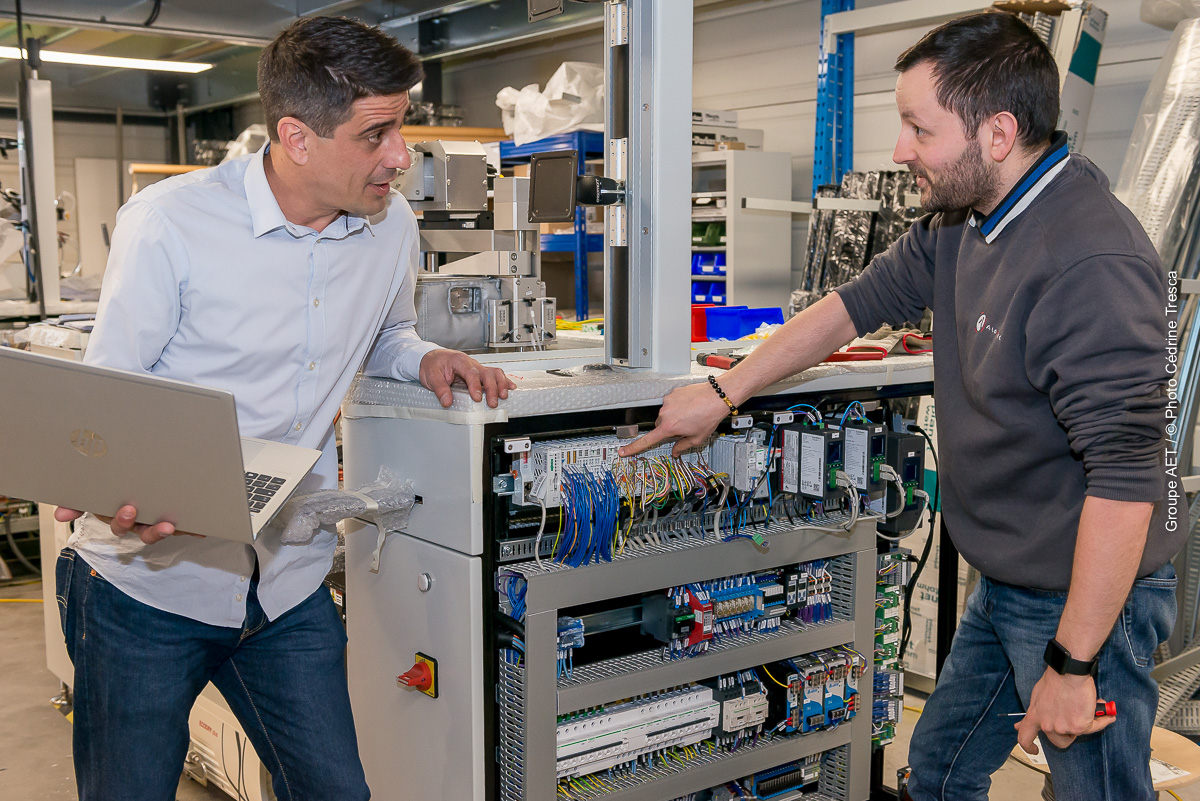
The common requirement across all five technology domains is process control that is physically grounded, measurable in real time and repeatable at wafer scale. The ALOXTEC portfolio addresses this with a unified T/H/P process architecture, a full-wafer in-situ vision system on every machine, Stop-on-Aperture endpoint control, and UniformPerf© spatial uniformity compensation as a validated production option.
The same equipment serves Tier 1 volume production lines and research and development environments, with full recipe portability that preserves process knowledge from device qualification through production ramp. Whether the challenge is a 3 µm aperture single-mode VCSEL, an EEL current-blocking oxide requiring long-term delamination resistance, or an AlOx waveguide cladding layer for a photonic integrated circuit, the process control requirements converge on the same engineering answer.
Contact our team to discuss your specific oxidation challenge, or explore the technology pages to find the detailed technical content relevant to your device and process context.
 Save as PDF