

In wet thermal oxidation of III-V semiconductors, the oxide aperture is not simply one parameter among many. It is the central geometric feature from which every electro-optical characteristic of the device derives. Its diameter sets the threshold current. Its position within the cavity determines the emission wavelength through the effective refractive index. Its shape governs beam symmetry and mode quality. Its interface integrity determines how long the device will operate reliably in the field.
Controlling this aperture with deterministic precision, on every wafer, across every run, and across the full surface of a 6-inch or 8-inch wafer, is the central engineering problem of III-V device manufacturing. This page explains why conventional timed oxidation cannot solve it, what the physical limits of that approach are, and how the ALOXTEC Stop-on-Aperture system replaces it with a fundamentally different process control paradigm.
The hardware architecture of ALOXTEC’s in-situ vision system, which enables Stop-on-Aperture, is described in detail on the Real-Time In-Situ Monitoring System page. This page focuses on the process control logic, the failure modes it eliminates, and its quantitative implications for yield and production stability.
The oxide aperture is defined by four geometric parameters, each of which controls a distinct axis of device performance. Understanding this four-dimensional relationship is the starting point for understanding why aperture control is the single most leveraged intervention in VCSEL and EEL process engineering.
| Aperture parameter | Physical significance | Process control lever |
|---|---|---|
| Aperture diameter | The primary yield-determining parameter. Controls threshold current, slope efficiency and, through effective refractive index, emission wavelength. | Controlled by the Stop-on-Aperture endpoint: the process terminates when the target diameter is reached (max 3 µm with the ALOXTEC equipment), regardless of elapsed time or run-to-run rate variation. |
| Aperture circularity | The roundness of the oxide aperture determines beam symmetry and far-field mode quality. Non-circular apertures produce elliptical or asymmetric beam profiles, which degrade coupling efficiency into circular optical fibres and create beam quality issues in LiDAR applications. | Circularity is influenced by the spatial symmetry of the T/H/P field within the chamber. UniformPerf© active thermal gradient compensation improves aperture circularity as a direct consequence of homogenising the oxidation environment. |
| Oxide transition sharpness | The abruptness of the AlGaAs/AlOx transition at the aperture boundary determines optical scattering losses and mode quality. A gradual transition produces a graded refractive index profile at the aperture edge, affecting mode confinement. | Transition sharpness is primarily a function of water vapour activity and temperature. Water-limited oxidation conditions, as used in the ALOXTEC process, tend to produce sharper, more abrupt transitions than high-water-activity processes. |
| Wafer-level aperture uniformity | The spatial distribution of aperture diameters across the full 6-inch or 8-inch wafer is the direct determinant of binnable yield. Uniformity is quantified as the min-max spread across a standard measurement grid with 5 mm edge exclusion. | Uniformity is addressed through two complementary mechanisms: Stop-on-Aperture ensures that the global mean aperture is correct; UniformPerf© addresses the spatial gradients that cause die-to-die variation around that mean. |

The economic implications of aperture non-uniformity are direct and quantifiable. At the scale of high-volume consumer electronics or AI datacom VCSEL production, a single 6-inch wafer may contain tens of thousands of individual VCSEL dies. The fraction of those dies that fall within the specification window for threshold current, wavelength and modulation bandwidth is a direct function of how tightly the aperture diameter is controlled across the wafer.
Every additional 0.1 µm of aperture uniformity error reduces the fraction of in-specification dies by a measurable amount. The relationship is not linear: near the edges of a specification window, small improvements in uniformity produce disproportionately large gains in binnable yield because they move the tails of the aperture distribution inside the pass band. At the volumes characteristic of consumer electronics and AI infrastructure deployment, each yield point per wafer translates directly into a measurable change in cost per good die, and cost per good die is the primary competitive parameter in volume photonic component manufacturing.
In a conventional wet oxidation furnace, the process is stopped based on a predetermined time calculated from a calibrated oxidation rate established during process qualification. This approach contains a structural incompatibility with the requirements of high-yield VCSEL production: it assumes that the oxidation rate is a stable, reproducible constant. It is not.
The lateral oxidation rate in a wet thermal oxidation furnace is a function of at least four independently varying quantities: local temperature at the wafer surface, local water vapour concentration at the oxidation front, Al mole fraction in the target epitaxial layer, and the progressive change in chamber conditioning state over the course of a production campaign. None of these quantities is perfectly constant. Each of them introduces an independent contribution to run-to-run and die-to-die aperture variability that a time recipe, however carefully optimised, cannot compensate in real time.
The table below maps the four primary sources of timed oxidation variability to their physical mechanisms and process consequences.
| Source of variability | Physical mechanism | Process consequence |
|---|---|---|
| Local temperature gradients within the furnace chamber | The oxidation rate is an exponential function of temperature. Even a fraction of a degree of spatial non-uniformity across the wafer surface produces a measurable difference in local oxidation rate from die to die. | Aperture diameter varies across the wafer. Dies at hotter regions of the wafer develop larger apertures than dies at cooler regions, creating a systematic, thermally-driven yield loss that a time recipe cannot compensate. |
| Run-to-run variation in water vapour delivery | Water vapour flow rate and its spatial distribution within the chamber are subject to calibration drift, temperature-dependent carrier gas saturation variation, and changes in chamber surface condition over time. | The same time recipe produces apertures of different sizes in consecutive runs. Production margins must be widened to accommodate this drift, reducing yield and increasing the risk of systematic over- or under-oxidation. |
| Incoming EPI Al content variability | Lateral variations in Al mole fraction within the target AlGaAs layer, arising from epitaxial growth non-uniformity, produce corresponding local variations in oxidation rate that are independent of furnace conditions. | A time recipe optimised for one EPI lot may over-oxidise or under-oxidise the next. This makes the oxidation process sensitive to incoming material quality in a way that cannot be corrected within the process step. |
| Chamber conditioning state | The thermal and chemical state of the furnace chamber changes gradually over time as a function of run history, cleaning cycle frequency and process recipe sequence. | Oxidation rate drifts systematically between maintenance cycles. Without real-time endpoint detection, this drift accumulates into a yield offset that shifts unpredictably between production lots. |

The three failure modes that result from inadequate aperture control each carry specific and distinct consequences for device performance and production economics.
| Deviation type | Physical consequence | Production impact |
|---|---|---|
| Over-oxidation (aperture too small) | The current-confining aperture is reduced below the target diameter. Threshold current increases beyond specification. For small-aperture single-mode VCSELs, over-oxidation can completely close the optical mode, rendering the device non-functional. | Device fails electrical test. No downstream process step can recover a closed or under-sized aperture. The entire wafer represents unrecoverable scrap. In high-pressure oxidation processes, over-oxidation is the primary cause of catastrophic yield loss events. |
| Under-oxidation (aperture too large) | The oxide does not extend far enough from the mesa edge. Current confinement is insufficient, resulting in elevated threshold current, reduced slope efficiency, multi-mode emission, and degraded high-speed modulation bandwidth. | Device fails specification on threshold current, emission wavelength or modulation performance. Binnable yield is reduced. In wavelength-division multiplexed applications (datacom, LiDAR), aperture size directly controls the emission wavelength, making under-oxidation a channel alignment risk. |
| Non-uniform aperture (size gradient across wafer) | Even when the mean aperture size is correct, a spatial gradient in aperture diameter across the wafer creates a population of devices with distributed threshold currents and wavelengths. Devices at the wafer edge and centre have different electrical and optical characteristics. | Only a fraction of dies fall within the specification window. Binnable yield is directly proportional to aperture uniformity. At 6-inch wafer scale, every 0.1 µm of additional uniformity error corresponds to a measurable reduction in the fraction of dies meeting the tightest specification bins. |
The critical insight is that none of these failure modes can be corrected downstream. A VCSEL die with an incorrect aperture diameter cannot be reworked. An over-oxidised device that has lost its optical mode is unrecoverable. A wafer with high aperture non-uniformity cannot be sorted into a uniform bin. The only effective intervention is at the process step itself, with real-time control that eliminates the deviation before it occurs.
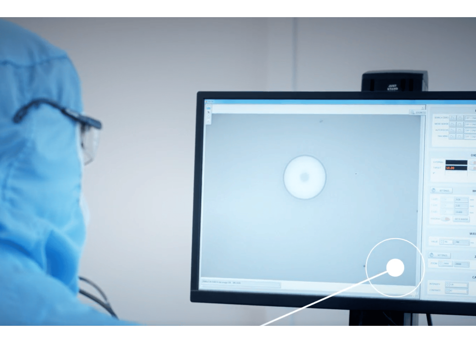
The ALOXTEC Stop-on-Aperture function replaces the timed oxidation paradigm entirely. Rather than inferring the process endpoint from a pre-calibrated time and rate model, the system measures the actual aperture size directly, continuously and in real time as the oxidation proceeds, then terminates the process automatically when the measured aperture reaches the target diameter.
This represents a fundamental change in process control architecture. The process endpoint is no longer inferred from a model that may or may not reflect the actual run conditions. It is measured, directly, on the actual device structures, on the actual wafer, in the actual furnace environment of the run in progress. The result is deterministic endpoint control that is, by construction, independent of run-to-run variations in oxidation rate, EPI Al content variability, chamber conditioning drift or water vapour delivery fluctuation.
The Stop-on-Aperture control sequence unfolds across five stages, from run initialisation through post-oxidation characterisation. Each stage is described below in terms of what the system does and the decision logic it applies.
| Process stage | What the system does | Decision logic |
|---|---|---|
| Run initialisation | The in-situ vision system scans the wafer surface and identifies all mesa structures using automatic pattern recognition. No operator input or manual template definition is required. | Mesa coordinates, dimensions and expected oxidation directions are registered. The system establishes the baseline measurement reference for each die across the full wafer. |
| Active oxidation phase | The vision system monitors the advancing oxidation front continuously across the full wafer surface. Both low-magnification (wafer-level overview) and high-magnification (mesa-level resolution) channels operate simultaneously throughout the run. | The oxidation front position is computed in real time for each monitored mesa. The system tracks the instantaneous aperture size as the oxide advances inward from the mesa edge. |
| Approaching target aperture | As the measured aperture approaches the target diameter, the system transitions to higher-frequency measurement and increased sensitivity. The rate of aperture closure is tracked and used to project the time-to-endpoint. | The endpoint projection enables the system to initiate the process termination sequence with the precise lead time required for the furnace to respond, accounting for the thermal and gas-flow inertia of the chamber. |
| Endpoint and process termination | When the target aperture size is reached at the monitored reference mesas, the Stop-on-Aperture algorithm triggers the automatic process termination sequence: water vapour is removed from the chamber and the thermal ramp-down begins. | Termination is triggered by measured aperture size, not by elapsed time. The process stops at the same aperture diameter regardless of run-to-run variations in oxidation rate, EPI Al content variability, or chamber conditioning state. |
| Post-oxidation characterisation | With the wafer still in the chamber, the vision system performs a full characterisation sweep: oxidation depth map, aperture size map, circularity index, mesa size map and emitting wavelength map across the full wafer. | Complete process quality data is available before the wafer leaves the chamber. Uniformity deviations are identified immediately, on the current wafer, enabling instant process feedback without a separate metrology step. |
The Stop-on-Aperture system is capable of targeting aperture diameters down to 3 µm, covering the full range of aperture sizes used in commercial VCSEL and EEL manufacturing. The target aperture is defined in the process recipe and can be adjusted without any hardware modification or system recalibration.
This flexibility allows the same ALOXTEC system to be used across a wide range of device types and epitaxial structures, with process recipes that transfer directly between the GEN1.4L Manual, GEN1.4L Auto and GEN2.0 HV Auto equipment without tool-specific requalification. The process recipe developed on a research system is the process recipe that runs in production.

Stop-on-Aperture is a global process control function. It controls the mean aperture size across the wafer with high accuracy, ensuring that the process terminates at the correct average aperture diameter regardless of run-to-run rate variability. It does not, by itself, eliminate the spatial aperture gradients within the wafer that arise from temperature and water vapour non-uniformity within the furnace chamber.
These two control problems, mean aperture accuracy and wafer-level spatial uniformity, are distinct in their physical origin and require different engineering solutions. Stop-on-Aperture addresses the first. UniformPerf©, ALOXTEC’s patented hardware and software option, addresses the second by acting on the root causes of spatial non-uniformity: local temperature gradients and water vapour distribution gradients within the chamber.
When Stop-on-Aperture and UniformPerf© operate together, they address the full scope of aperture control requirements in high-volume VCSEL production:
The UniformPerf© technology, its hardware architecture, the physical mechanisms it addresses and its validated performance data are described in detail on the UniformPerf© Technology page.

The Stop-on-Aperture control architecture is device-agnostic. It operates identically for VCSEL structures and edge-emitting laser structures, for small-aperture single-mode devices and large-aperture multi-mode or high-power arrays, and across the full range of AlGaAs epitaxial structures encountered in III-V device manufacturing.
The system does not rely on a device-specific calibrated rate model. It measures the actual oxidation front on the actual device structures of each wafer in real time. This means that a change in epitaxial structure, a new EPI supplier, or a process recipe development run on a new device geometry does not require re-establishing a calibrated time endpoint. The system adapts to the actual oxidation behaviour of each wafer automatically, without any operator intervention.
This property is particularly valuable in research and development environments, where epitaxial structures change frequently, and in production environments where multiple product families are processed on the same system. The ALOX GEN1.4L Manual is routinely used in this mode, providing the same Stop-on-Aperture endpoint control on novel research structures that the GEN1.4L Auto provides in automated production environments.
Oxide aperture control is the most critical process step in VCSEL manufacturing, directly determining yield, performance and production stability. Unlike conventional furnace approaches based on time estimation, advanced oxidation control relies on real-time measurement and feedback. The following questions address the key mechanisms, limitations and innovations in aperture control technologies.
 Save as PDF