
Pre-sales open
For VCSELs quality control
As demand for high-quality VCSELs accelerates across datacom, 3D sensing, automotive, and industrial applications, leading manufacturers are strengthening their quality control capabilities both upstream and downstream of the VCSEL wet thermal oxidation process.
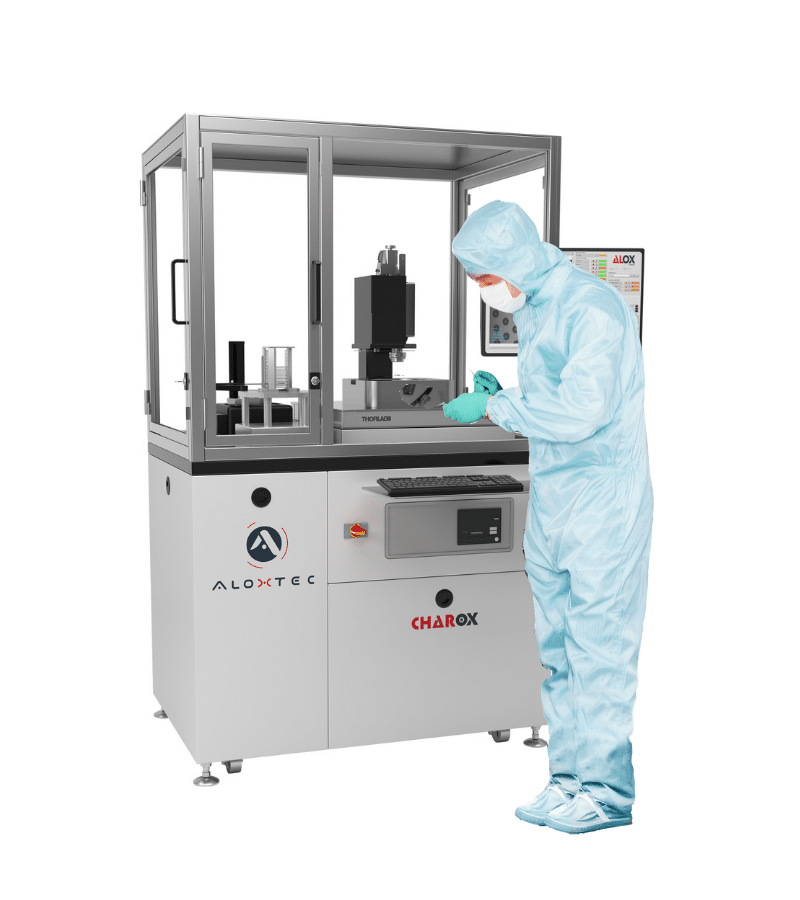
The CHAROX 1.0 is ALOXTEC’s answer: a solution exclusively dedicated to wafer characterization, available in manual or automated configurations, while delivering the same characterization performance as that integrated into our ALOX GEN 1.4L Manual , ALOX GEN 1.4L Automatic, and ALOX GEN2.0 HV Auto equipment.
60+ tools used worldwide in 21 customers sites
Support and Sales representatives in EU, Asia & US
| Specification | Value |
|---|---|
| Throughput | Contact ALOXTEC’s team |
| Wafer sizes | 3” to 8” |
| Loading |
|
| Proprietary vision system |
|
| Supervision and vision software |
|
| Availability | Presales open, contact ALOXTEC for configuration and lead time |

The CHAROX 1.0 characterisation tool enables full-wafer, die-level inspection prior to wet oxidation, transforming incoming wafer qualification into a quantitative, spatially resolved dataset. The mesa size map provides a complete geometric characterisation of each structure across the wafer, capturing etch dimensions, shape and positional accuracy with ultra-high measurement resolution. This dataset acts as a pre-oxidation reference, allowing process engineers to identify lithography and etch non-uniformities before they propagate into oxidation-induced variability. Variations detected at this stage are not attributable to the oxidation step, enabling immediate isolation of upstream process deviations. As a result, pre-oxidation characterisation becomes a structured quality gate for EPI wafers, reducing the risk of introducing non-conforming material into the oxidation process.
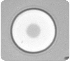
Following wet oxidation, the CHAROX 1.0 generates a complete characterisation sweep across the full wafer surface, producing five simultaneous measurement outputs: oxidation depth, aperture size, circularity, mesa geometry and emitting wavelength.Each output captures a distinct dimension of process and device quality, and together they form a spatially resolved dataset at die level. This dataset does not provide a summary indicator, but a quantitative reconstruction of the oxidation outcome across the wafer:
The result is a complete and coherent view of process outcome, enabling immediate assessment of uniformity, performance distribution and specification compliance across the entire wafer.

The simultaneity of the five measurement outputs enables a diagnostic capability that extends beyond the oxidation step itself. Because all datasets are acquired on the same wafer, within the same spatial reference frame, correlations and non-correlations between outputs carry direct information about process origin. An aperture gradient that correlates with an oxidation depth gradient indicates a process-induced non-uniformity, typically linked to temperature, water vapour or pressure conditions. The same aperture variation without corresponding depth variation reveals a material-driven deviation, such as local EPI composition differences. The mesa size map provides a direct reference to upstream lithography and etch quality, enabling cross-step analysis across the fabrication flow. This structured interpretation framework transforms characterisation into a process diagnostic tool, directing corrective action to the appropriate step: oxidation, EPI growth or upstream patterning.
The aperture size map generated by the CHAROX 1.0 provides a direct, quantitative link between process output and device performance, making it the primary wafer-level yield predictor. Each die is assigned a measured aperture diameter that can be compared against specification windows for threshold current, emission wavelength and modulation performance. Dies within specification are predicted to pass electrical test, while out-of-specification dies are identified at the characterisation stage. This enables early yield estimation, prior to downstream testing, and supports informed lot disposition decisions. In addition, the structured dataset can be integrated into statistical process control frameworks, where run-to-run metrics such as mean aperture, aperture spread and wafer-level uniformity are trended over time. This transforms characterisation from a measurement step into a decision framework, supporting both immediate process control and long-term yield optimisation.



 Save as PDF