

Silicon Photonics provides the passive infrastructure. III-V semiconductors provide the light. Wet thermal oxidation is the process that connects them.
About Silicon Photonics and III-V Wet Thermal Oxidation

Silicon Photonics has fundamentally redefined the economics of optical communication. The ability to fabricate passive optical components, including waveguides, ring resonators, arrayed waveguide gratings, and grating couplers, using the same CMOS foundry infrastructure developed for microelectronics has driven dramatic reductions in the cost and power consumption of optical transceivers. Today, Silicon Photonics dominates the market for datacenter optical interconnects, with multiple high-volume foundries producing SiPho chips at wafer scale for 400G and 800G transceiver applications.
However, Silicon Photonics carries a fundamental materials limitation that no amount of process engineering can overcome: silicon is an indirect bandgap semiconductor. Its radiative recombination efficiency is negligible, which means that silicon cannot generate or amplify light efficiently. Every Silicon Photonics chip that operates as an active optical transceiver requires an external or heterogeneously integrated light source, and that light source must come from a III-V semiconductor, typically based on GaAs/AlGaAs or InP/InGaAsP material systems, where direct bandgap transitions support efficient laser emission and optical amplification.
The integration of III-V active components onto Silicon Photonics systems is therefore not an optional performance enhancement: it is a structural necessity for any SiPho chip that must generate or amplify light. As the industry moves from pluggable optical modules toward co-packaged optics (CPO), in which the optical engine is integrated directly alongside the switch ASIC or GPU on the same package substrate, the III-V/Si heterogeneous integration challenge moves from the module level to the chip level, placing new and more demanding requirements on the III-V component fabrication processes involved.

In III-V components designed for integration onto Silicon Photonics systems, wet thermal oxidation of AlAs or AlGaAs layers serves two critical functions that cannot be replicated by any other semiconductor fabrication process. The first is current confinement in laser sources and amplifiers: the AlOx aperture produced by selective wet oxidation provides the lateral current-confining structure that defines the threshold current, emission wavelength, and output power of the on-chip III-V laser or semiconductor optical amplifier. Without a precisely controlled oxide aperture, the III-V active component cannot meet the power efficiency and wavelength stability requirements of co-packaged optics applications. The second function is optical confinement in waveguide coupler structures: in the transition regions where the III-V waveguide mode must be adiabatically transferred to the silicon photonics waveguide, the AlOx cladding provides the high-index-contrast boundary conditions that define the mode profile and group index of the III-V waveguide, and hence the phase-matching condition at the III-V/Si coupler interface.
In both cases, the precision of the wet oxidation process translates directly into the performance and yield of the integrated III-V/SiPho device. Small aperture size deviation errors in oxide aperture size or cladding depth propagate into threshold current deviations, wavelength offsets, and coupler transmission losses that degrade the system-level performance of the co-packaged optics engine.
The table below maps the functional requirements of a Silicon Photonics system against the respective capabilities of silicon and III-V materials, identifying specifically where wet thermal oxidation of III-V layers is a required process step:
| SiPho system function | Silicon photonics capability | III-V wet oxidation contribution |
|---|---|---|
| Light generation | Not possible: silicon is an indirect bandgap semiconductor with negligible radiative recombination efficiency | AlGaAs/GaAs or InP/InGaAs lasers with AlOx current-confining apertures provide the on-chip light source |
| Optical amplification | Not achievable in Si or SiO2: no optical gain mechanism available at telecom or datacom wavelengths | III-V semiconductor optical amplifiers (SOAs) with AlOx waveguide cladding provide on-chip gain for signal conditioning and booster stages |
| High-speed electro-optic modulation | Possible via plasma dispersion effect in Si, but limited by carrier lifetime and free-carrier absorption loss at high speed | III-V electro-absorption modulators with AlOx waveguide confinement offer higher bandwidth and lower drive voltage than Si plasma modulators |
| Passive routing, splitting and filtering | High performance: ring resonators, AWGs, MMI couplers, grating couplers all well established in Si/SiO2 | No III-V oxidation required for passive Si functions: Si photonics handles this natively |
| Photodetection | Germanium-on-silicon photodetectors cover O, C and L bands and are well integrated in SiPho foundry flows | III-V InGaAs photodetectors offer extended wavelength range and higher responsivity for specific applications beyond the Ge-on-Si coverage |
The practical implication of this mapping is that any Silicon Photonics system targeting co-packaged optics, optical transceivers, LiDAR on chip, or coherent optical communication must incorporate III-V components for at least the light generation and amplification functions, and those components must be fabricated with a wet thermal oxidation step that defines their current-confining aperture or waveguide cladding structure.
The process control requirements for wet thermal oxidation in a Silicon Photonics integration context combine elements from all three other ALOXTEC application domains: the aperture size precision and yield economics of VCSEL manufacturing, the wavelength stability requirements of EEL-based transceivers, and the ultra-precise depth control requirements of III-V waveguide fabrication. Three requirements stand out as particularly demanding in the SiPho context.

Co-packaged optics and photonic integration applications impose strict constraints on the physical footprint of every component on the chip. III-V laser sources and amplifiers designed for heterogeneous integration onto Silicon Photonics systems are typically fabricated with mesa widths and aperture dimensions significantly smaller than those used in stand-alone VCSEL or EEL products, in order to minimise the area of the III-V die that must be bonded or transferred onto the silicon substrate. For a laser with a target aperture of 3 µm, real-time Stop-on-Aperture control is essential — and only the ALOXTEC in-situ vision system delivers that level of precision.
At these small aperture dimensions, the sensitivity of the oxidation rate to local temperature gradients and EPI Al content variations is at its highest, making timed-oxidation approaches fundamentally incompatible with the yield requirements of SiPho-integrated III-V components. The ALOXTEC Stop-on-Aperture function, which terminates the process at the exact target aperture size based on real-time measurement rather than a pre-calibrated time constant, is not a performance advantage in this context: it is a prerequisite for achieving acceptable yield.

III-V components designed for heterogeneous integration onto Silicon Photonics systems are typically built from significantly more complex epitaxial structures than stand-alone VCSELs or EELs. A III-V/Si integration stack may include an etch stop layer, a bonding interface layer, the active quantum well region, multiple cladding layers with different Al contents, a current-spreading layer, and a contact layer,All contained within an epitaxial layer of infinitesimal thickness. In this complex stack, the Al-containing layer targeted for wet oxidation may be flanked above and below by layers with different Al contents and different susceptibilities to lateral oxidation, requiring precise control of the T/H/P (Temperature / Humidity / Pressure) conditions to achieve selective oxidation of the intended layer without unintended oxidation of adjacent Al-containing layers.
The ALOXTEC T/H/P (Temperature / Humidity / Pressure) process window, spanning 350 to 600 °C in temperature, 0.6 to 30 g/h in water flow, and a few millibar to Pa, provides sufficient parameter space to configure and optimise oxidation recipes for a wide range of customer-specific epitaxial structures. Based on the customer wafer design and process objectives, ALOXTEC supports users in defining the appropriate oxidation conditions required to selectively target the intended Al-containing layer while preserving adjacent lower-Al layers. This process-driven approach enables customers to efficiently transfer and adapt their own III-V/Si integration architectures onto the ALOXTEC equipment.

Co-packaged optics systems deployed in AI training clusters and hyperscale datacenter switching fabrics are expected to operate continuously for multiple years, with mean times between failure measured in millions of hours per port. The thermal environment inside a co-packaged optics engine is significantly more demanding than that of a pluggable optical module: the III-V components are mounted directly adjacent to high-power CMOS die that dissipate watts, creating junction temperature excursions and thermal cycling amplitudes that are more severe than those encountered in any previous optical transceiver application.
In this thermal environment, the structural integrity of the AlGaAs/AlOx interface in every III-V active component becomes a critical reliability determinant. The ALOXTEC low-pressure oxidation process, which minimises arsine entrapment and volumetric expansion stress at the AlGaAs/AlOx interface, and the integrated post-oxidation annealing step, which relaxes residual interfacial stress before the wafer cools, together produce oxide layers with demonstrably superior resistance to thermomechanical delamination under the accelerated thermal cycling conditions used to qualify co-packaged optics components. For SiPho customers building qualification packages for hyperscale datacenter customers, the process provenance of the wet oxidation step is a relevant factor in the reliability case.
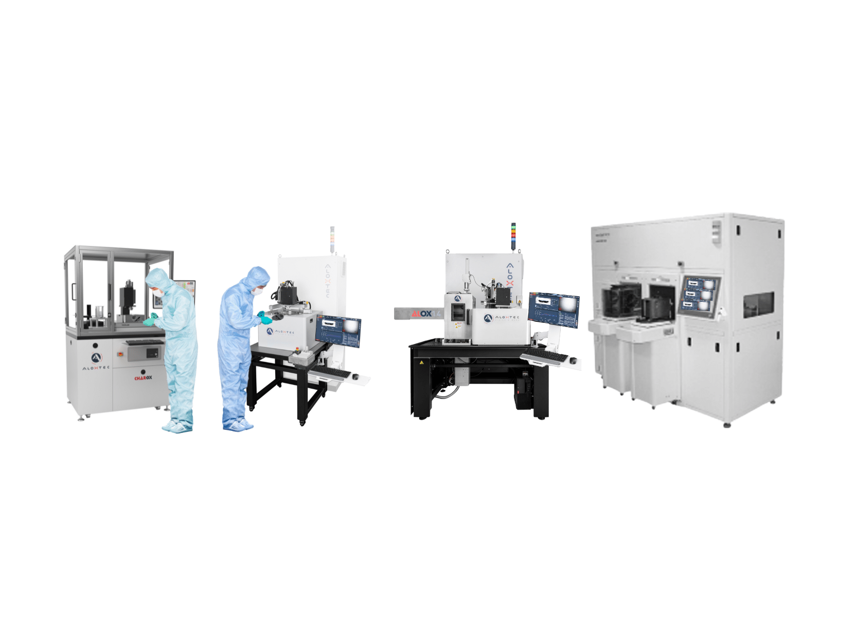
Silicon Photonics integration programmes typically evolve through a well-defined sequence of development stages, from initial epitaxial design and process exploration through device qualification to foundry-scale production. The ALOXTEC product range covers this full lifecycle because every equipment shares the same process chamber geometry, gas delivery architecture, and in-situ vision system, ensuring complete recipe portability at every transition point.
| Development stage | Environment | Recommended ALOXTEC equipment | Key capability |
|---|---|---|---|
| Concept & epitaxial design | University cleanroom, national lab | ALOX GEN1.4L Manual | Full T/H/P (Temperature / Humidity / Pressure) process window, in-situ depth measurement, manual flexibility for exploratory DOE |
| Process development & qualification | Industrial R&D fab, pilot line | ALOX GEN1.4L Auto or GEN1.4L Manual | Automated runs for DOE efficiency, Stop-on-Depth, UniformPerf© option for wafer-level uniformity qualification |
| Process validation & metrology | Production QC, process control lab | CHAROX 1.0 | Dedicated oxide layer metrology system: depth mapping, uniformity analysis, without occupying the oxidation furnace |
| Volume production scale-up | Tier 1 SiPho foundry or IDM | ALOX GEN1.4L Auto or GEN2.0 HV Auto | 800 to 2,400 wafers/month, SECS/GEM integration, 100% recipe portability from GEN1.4 development systems |
The CHAROX 1.0 characterisation equipment deserves specific mention in the Silicon Photonics context. Process validation in SiPho integration flows typically requires detailed oxide layer metrology on a larger fraction of production wafers than in standard VCSEL manufacturing, because the consequences of an out-of-specification oxide depth are more severe in a multi-component integrated circuit than in a discrete device. The CHAROX 1.0 provides the same five-output characterisation capability as the in-furnace ALOXTEC equipment, depth map, aperture size map, circularity index, mesa size map, and emitting wavelength map, on a dedicated vibration-isolated optical bench, enabling high-throughput production QC without consuming furnace chamber time.
ALOXTEC’s engagement with the Silicon Photonics ecosystem is grounded in the same scientific partnerships that underpin the broader ALOXTEC equipment capability. The LAAS-CNRS, UC Berkeley Marvell NanoLab, Cardiff University and many others collaborations all include work on III-V/Si integration topics, including the fabrication and characterisation of AlOx-clad waveguide structures for coupling to silicon photonics passive circuits, the reliability of AlGaAs/AlOx interfaces under the thermal cycling conditions representative of co-packaged optics environments, and the development of oxidation process recipes for complex multi-layer III-V/Si integration stacks.

The Silicon Photonics industry is currently at an inflection point: the first generation of co-packaged optics products is entering mass production qualification, and the wet oxidation process step for the III-V active components is transitioning from a research-scale, manually operated furnace environment to an automated, SECS/GEM-integrated production flow. ALOXTEC’s experience in supporting this type of R&D to production transition, accumulated over 15 years and more than 60 equipment installations at VCSEL and EEL manufacturers, is directly applicable to the SiPho III-V integration context.
The ALOX GEN1.4L Auto and GEN2.0 HV Auto furnace provide the automation, throughput, and factory integration capabilities required for SiPho foundry environments, while the recipe portability from the GEN1.4L Manual and Auto development systems ensures that process knowledge developed during the R&D phase transfers directly to production without requalification cost. For Silicon Photonics customers building their III-V wet oxidation capability for the first time, ALOXTEC’s application engineering team provides structured process transfer support, DOE-based recipe development, and qualification documentation aligned with the customer’s quality management system.
The combination of Stop-on-Aperture automation, three-parameter T/H/P (Temperature / Humidity / Pressure) process control, UniformPerf© wafer-level uniformity, low-pressure reliability architecture, and integrated 3-in-1 oxidation, characterisation and annealing capability positions the ALOXTEC product range as the most complete and most precisely controlled wet oxidation solution available for III-V components in Silicon Photonics applications. No other wet oxidation equipment on the market combines real-time aperture measurement with the low-pressure process architecture required for co-packaged optics reliability, the multi-EPI experience needed for complex III-V/Si integration stacks, and the full production automation and SECS/GEM integration demanded by SiPho foundry environments.
Frequently Asked Questions about Silicon Photonics and III-V Wet Thermal Oxidation
Silicon photonics systems rely on the integration of III-V semiconductors to provide active optical functions such as light generation and amplification. In this hybrid architecture, wet thermal oxidation becomes a critical process step, defining both electrical and optical confinement within III-V components. The following questions address the key technical challenges of oxidation control in III-V/Si photonic integration.
 Save as PDF